Light-Emitting Element, Light-Emitting Device, Lighting Device, and Electronic Appliance

a technology of light-emitting elements and light-emitting devices, which is applied in the direction of thermoelectric devices, organic semiconductor devices, transistors, etc., can solve the problems of increasing shortening so as to improve the characteristics of the element, shorten the life of the element, and increase the driving voltage of an el element

Active Publication Date: 2015-11-05
SEMICON ENERGY LAB CO LTD
View PDF7 Cites 6 Cited by
  • Summary
  • Abstract
  • Description
  • Claims
  • Application Information

AI Technical Summary

Benefits of technology

[0010]As described above, the inverted-structure light-emitting element can be easily combined with the OS-FET and can be therefore expected to have better element characteristics than a conventional one. However, in the inverted-structure light-emitting element where an electron-injection layer, an electron-transport layer, and a light-emitting layer each including an alkali metal or an alkaline earth metal are stacked in this order over the cathode, contact of the electron-injection layer including an alkali metal or an alkaline earth metal with the already formed cathode, in particular, with a cathode including an oxide semiconductor transparent conductive film, increases the driving voltage of an EL element and shortens the lifetime of the element.

Problems solved by technology

However, in the inverted-structure light-emitting element where an electron-injection layer, an electron-transport layer, and a light-emitting layer each including an alkali metal or an alkaline earth metal are stacked in this order over the cathode, contact of the electron-injection layer including an alkali metal or an alkaline earth metal with the already formed cathode, in particular, with a cathode including an oxide semiconductor transparent conductive film, increases the driving voltage of an EL element and shortens the lifetime of the element.

Method used


Image

  • Light-Emitting Element, Light-Emitting Device, Lighting Device, and Electronic Appliance
  • Light-Emitting Element, Light-Emitting Device, Lighting Device, and Electronic Appliance
  • Light-Emitting Element, Light-Emitting Device, Lighting Device, and Electronic Appliance

Examples


embodiment 1

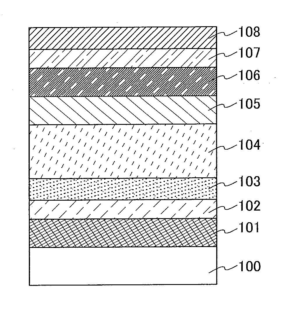
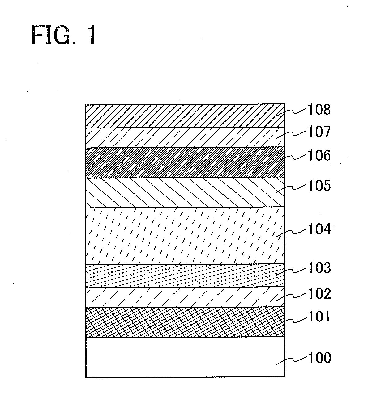
[0051]In this embodiment, a light-emitting element of one embodiment of the present invention will be described with reference to FIG. 1.

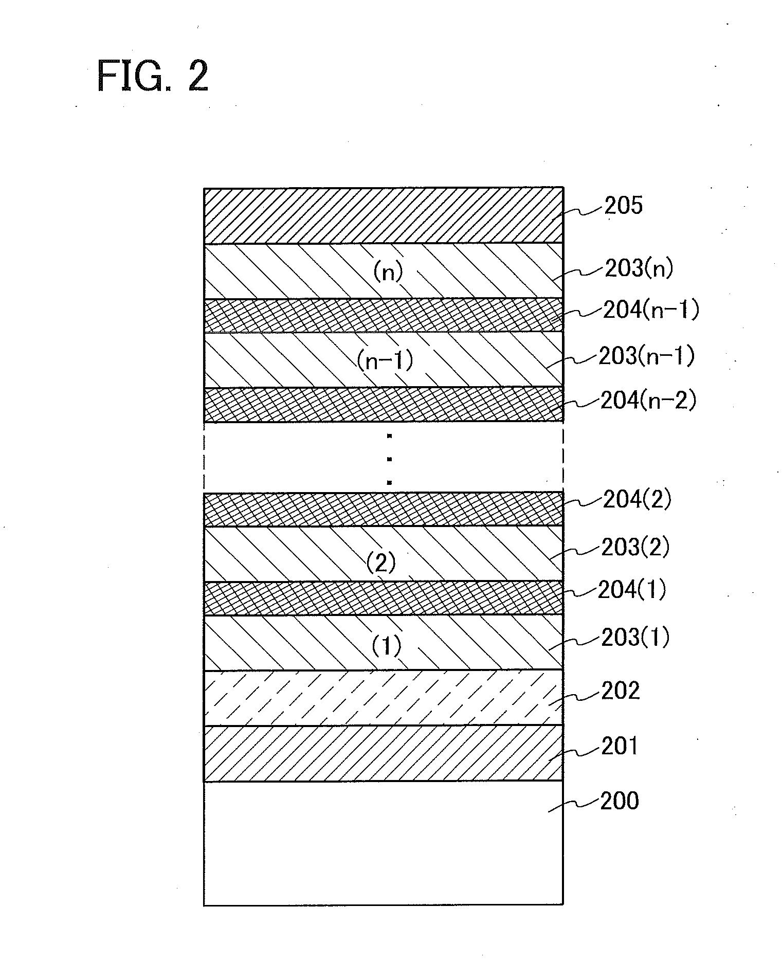
[0052]FIG. 1 illustrates an EL element in which an EL layer including a light-emitting layer 105 is provided between a cathode 101 and an anode 108. Although the number of EL layers is one in this embodiment, a tandem structure in which two or more EL layers are stacked may be employed. The cathode 101 is formed over a substrate 100; a layer 102 is formed over the cathode 101; an electron-injection layer 103 is formed over the layer 102; and an electron-transport layer 104, the light-emitting layer 105, a hole-transport layer 106, a hole-injection layer 107, and the anode 108 are formed in this order over the electron-injection layer 103; thus, the light-emitting element is formed. A field effect transistor (FET) may be formed between the substrate 100 and the cathode 101, and a signal supplied from the field effect transistor (FET) is input to the...

embodiment 2

[0093]In this embodiment, a light-emitting device including the light-emitting element described in Embodiment 1 will be described.

[0094]The light-emitting device may be either a passive matrix type light-emitting device or an active matrix type light-emitting device. The light-emitting element described in an embodiment other than Embodiment 1 can be applied to the light-emitting device described in this embodiment.

[0095]In this embodiment, an active matrix type light-emitting device is described with reference to FIGS. 3A and 3B.

[0096]FIG. 3A is a top view illustrating a light-emitting device and FIG. 3B is a cross-sectional view taken along the chain line A-A′ in FIG. 3A. The active matrix type light-emitting device according to this embodiment includes a pixel portion 502 provided over an element substrate 501, a driver circuit portion (a source line driver circuit) 503, and driver circuit portions (gate line driver circuits) 504a and 504b. The pixel portion 502, the driver circ...

embodiment 3

[0112]In this embodiment, examples of a variety of electronic appliances fabricated using a light-emitting device including the light-emitting element described in Embodiment 1 will be described with reference to FIGS. 4A to 4D.

[0113]Examples of electronic appliances that include the light-emitting device are television devices (also referred to as TV or television receivers), monitors for computers and the like, cameras such as digital cameras and digital video cameras, digital photo frames, cellular phones (also referred to as portable telephone devices), portable game consoles, portable information terminals, audio playback devices, large game machines such as pin-ball machines, and the like. Specific examples of these electronic appliances are illustrated in FIGS. 4A to 4D.

[0114]FIG. 4A illustrates an example of a television device. In a television device 7100, a display portion 7103 is incorporated in a housing 7101. Images can be displayed by the display portion 7103, and the ...


PUM


Abstract

An inverted-structure light-emitting element is provided. One embodiment of the invention disclosed in this specification is a light-emitting element including a cathode, a layer serving as a buffer over the cathode, an electron-injection layer over the layer serving as a buffer, a light-emitting layer over the electron-injection layer, and an anode over the light-emitting layer. The electron-injection layer includes an alkali metal or an alkaline earth metal. The layer serving as a buffer includes an electron-transport material. In the inverted-structure light-emitting element, contact of the alkali metal or alkaline earth metal included in a material of the electron-injection layer with the already formed cathode increases the driving voltage of an EL element and reduces emission efficiency. This problem becomes prominent particularly when the cathode includes an oxide conductive film. To prevent this, the layer serving as a buffer is provided between the cathode and the electron-injection layer.

Description

BACKGROUND OF THE INVENTION[0001]1. Field of the Invention[0002]One embodiment of the present invention relates to a light-emitting element.[0003]Note that one embodiment of the present invention is not limited to the above technical field. The technical field of one embodiment of the invention disclosed in this specification and the like relates to an object, a method, or a manufacturing method. In addition, one embodiment of the present invention relates to a process, a machine, manufacture, or a composition of matter. Specifically, examples of the technical field of one embodiment of the present invention disclosed in this specification include a semiconductor device, a display device, a liquid crystal display device, a light-emitting device, a lighting device, a power storage device, a storage device, a method for driving any of them, and a method for manufacturing any of them.[0004]2. Description of the Related Art[0005]Light-emitting elements utilizing electroluminescence have...

Claims


Application Information

Patent Timeline
Patent Type & Authority Applications(United States)
IPC IPC(8): H01L27/32H01L51/00H01L51/50H01L51/52H01L29/786H01L29/24
CPCH01L27/3248H01L2251/308H01L29/24H01L27/322H01L27/323H01L51/5072H01L51/5206H01L51/5234H01L51/0067H01L51/0072H01L51/0071H01L51/0085H01L2251/5353H01L2251/301H01L2251/306H01L29/7869H01L29/786H01L27/1225H10K85/615H10K85/631H10K85/6576H10K85/6572H10K85/342H10K50/171H10K59/123H10K50/16H10K50/11H10K50/81H10K50/82H10K50/828H10K59/38H10K59/40H10K85/654H10K85/657H10K2102/00H10K2102/102H10K2102/103H10K2102/321
Inventor KATAISHI, RIHOSASAKI, TOSHIKISEO, SATOSHI
Owner SEMICON ENERGY LAB CO LTD
Why Eureka
Try Eureka