Organic Light Emitting Diode Display Device and Driving Method Thereof

a light-emitting diode and display device technology, applied in semiconductor devices, instruments, electrical devices, etc., can solve the problems of low light emission efficiency, low brightness and high power consumption, and serious problems of pdps, so as to enhance the accuracy of compensation, accurate control of current flowing, and enhance the effect of compensation accuracy

Active Publication Date: 2015-11-12
LG DISPLAY CO LTD
View PDF20 Cites 25 Cited by
  • Summary
  • Abstract
  • Description
  • Claims
  • Application Information

AI Technical Summary

Benefits of technology

[0011]The embodiments relate to provide an organic light emitting diode display device and a driving method thereof which are adapted to detect a threshold voltage of a driving transistor and accurately control a current flowing through an organic light emitting diode.
[0012]Also, the embodiments relate to provide an organic light emitting diode display device and a driving method thereof which are adapted to enhance the accuracy of compensation through mobility detection of a driving transistor.
[0013]Moreover, the embodiments relate to provide an organic light emitting diode display device and a driving method thereof which are adapted to enhance the accuracy of compensation by eliminating error components which are caused by the capacitance of a capacitor on a sensing line and abnormal properties of elements.

Problems solved by technology

However, the PDPs have serious problems such as low light emission efficiency, low brightness and high power consumption.
However, the thin film transistor LCD devices have disadvantages such as a narrow viewing angle and a low response time, because of being non-luminous devices.

Method used


Image

  • Organic Light Emitting Diode Display Device and Driving Method Thereof
  • Organic Light Emitting Diode Display Device and Driving Method Thereof
  • Organic Light Emitting Diode Display Device and Driving Method Thereof

Examples


first embodiment

Detection of Mobility

[0115]FIG. 8 is a timing chart illustrating operational relations of switch elements at mobility detection according to a first embodiment of the present disclosure.

[0116]The mobility detection period can be defined into a second initialization interval Ti2, a second sensing interval Tse2 and a second sampling interval Tsa2.

Second Initialization Interval Ti2

[0117]The second initialization interval Ti2 is a period for initializing the first, second and third nodes A, B and C with a fixed voltage.

[0118]In the second initialization interval Ti2, the scan switch SW1 is turned-on in response to a scan pulse with a high level and the sensing switch SW3 is also turned-on in response to a sensing control signal SCS with the high level. As such, the initialization voltage Vinit on the sensing line S1 can be applied to the second node B, and simultaneously a second reference voltage Vref2 reflecting the detected threshold voltage Vth can be applied to the first node A.

[...

second embodiment

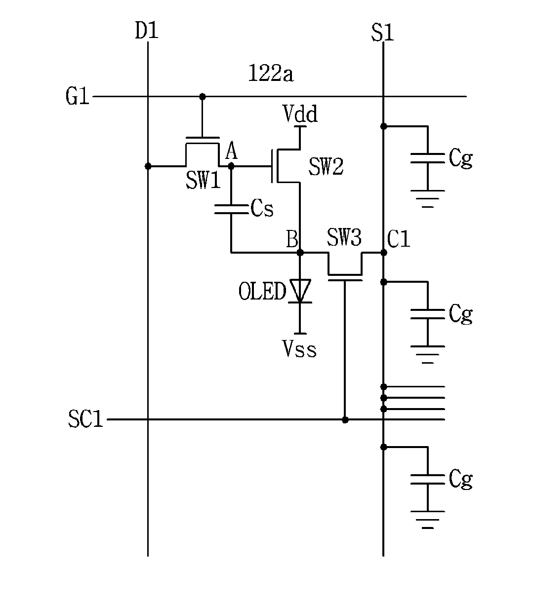
[0136]A driving method of an organic light emitting diode display device according to a second embodiment of the present disclosure can simultaneously compensate mobility difference between driving switches SW2 and parasitic or floating capacitance difference between the sensing lines S.

[0137]Connective configuration of sub-pixels arranged in a vertical direction will now be described with reference to FIG. 9. The sub-pixels include a first red sub-pixel 122a1, a second red sub-pixel 122a2 and an nth red sub-pixel 122an which are arranged in a horizontal direction. Scan switches SW1 of the first, second and nth red sub-pixels 122a1, 122a2 and 122an can be controlled by scan pulses on respective gate lines G1, G2 and Gn, input a data voltage from a first data line D1, and output sensing voltages through a first sensing line S1.

[0138]The first through nth red sub-pixels 122al-122an are sequentially driven by the scan pulses SP on the gate lines G1-Gn. As such, the sensing voltages for...


PUM


Abstract

An organic light emitting diode display device is disclosed which includes: a scan switch controlled by a scan pulse on a gate line and connected between a data line and a first node; a driving switch which includes a gate electrode connected to the first node, a source electrode connected to a second node, and a drain electrode connected to a first driving voltage line; a sensing switch controlled by a sensing control signal and connected between the second node and a third node on a sensing line; and an organic light emitting diode connected between the second node and a second driving voltage line.

Description

[0001]The present application claims priority under 35 U.S.C. §119(a) of Korean Patent Application No. 10-2014-0056584 filed on May 12, 2014, which is hereby incorporated by reference in its entirety.BACKGROUND[0002]1. Field of the Disclosure[0003]The present application relates to an organic light emitting diode display device and a driving method thereof.[0004]2. Description of the Related Art[0005]Recently, a variety of flat panel display devices with reduced weight and volume corresponding to disadvantages of cathode ray tube (CRT) are being developed. The flat panel display devices include liquid crystal display (LCD) devices, field emission display (FED) devices, plasma display panels (PDPs), electroluminescence devices and so on.[0006]The PDPs have advantages such as a simple manufacturing process, lightness and thinness, and easiness to provide a large-sized screen. In view of these points, the PDPs attract public attention. However, the PDPs have serious problems such as lo...

Claims


Application Information

Patent Timeline
Patent Type & Authority Applications(United States)
IPC IPC(8): G09G3/32
CPCG09G3/3241G09G2300/0852G09G2320/0233G09G2320/045G09G3/3233H10K59/00
Inventor YU, SANG HOKIM, TAE GUNGLEE, JONG MINLIM, MYUNG GIOH, HYE MISHIN, HUN KIYOON, JIN HAN
Owner LG DISPLAY CO LTD
Why Eureka
Try Eureka