

Flexible display substrate and a manufacturing method thereof, as well as a flexible display device
- Summary
- Abstract
- Description
- Claims
- Application Information
AI Technical Summary
Benefits of technology
Problems solved by technology
Method used
Image

Examples
Embodiment Construction
[0043]The technical solutions in the embodiments of the present invention will be described clearly and completely in combination with the drawings in the embodiments of the present invention in the following, apparently, the embodiments described below are only a part of rather than all of the embodiments of the present invention. Based on the embodiments in the present invention, all the other embodiments obtained by the ordinary skilled person in the art without paying any creative work belong to the protection scope of the present invention.
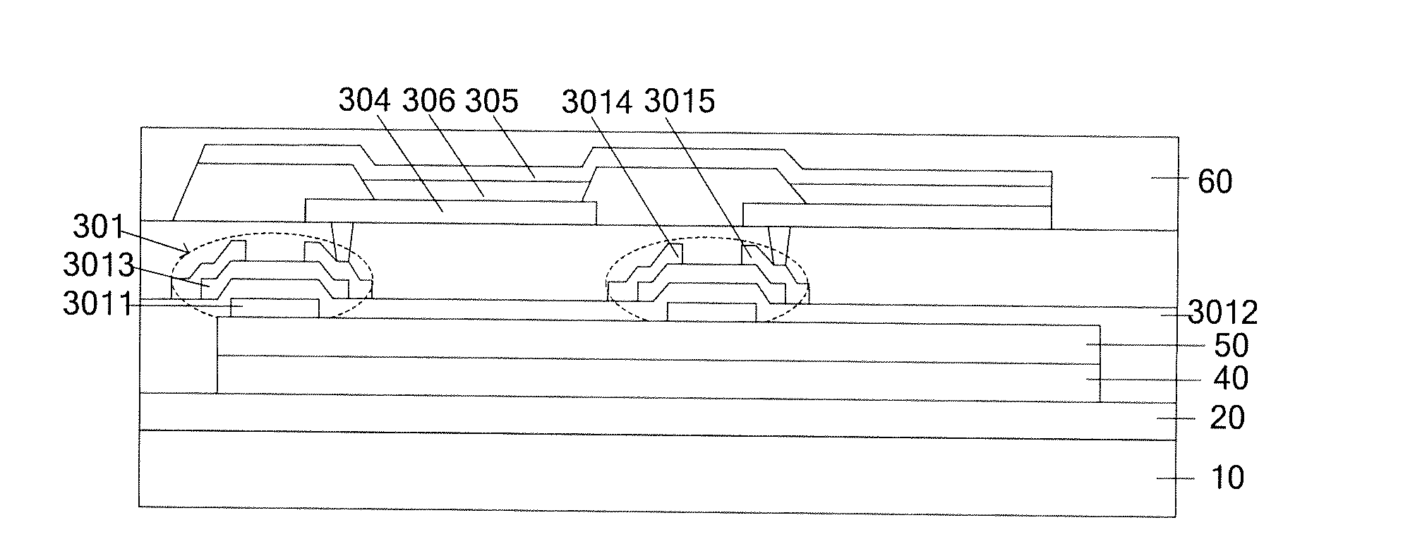
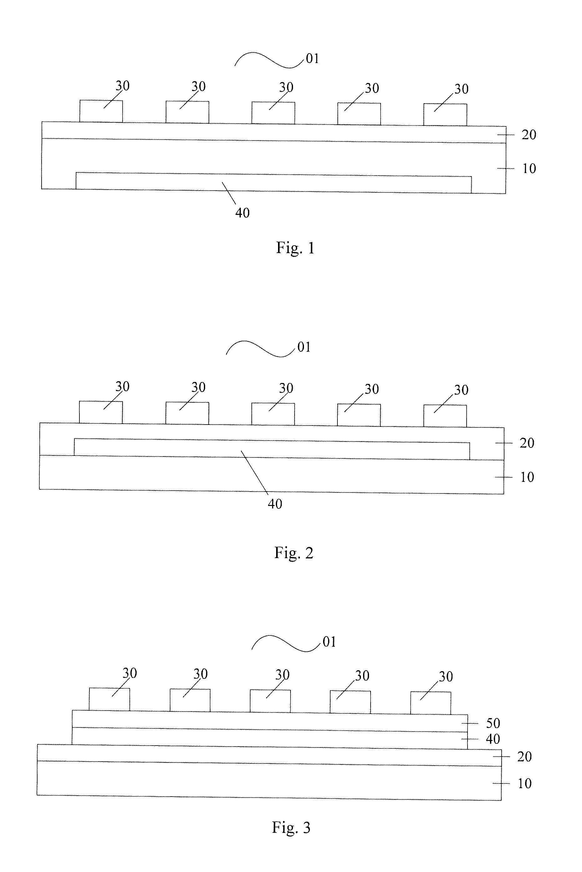
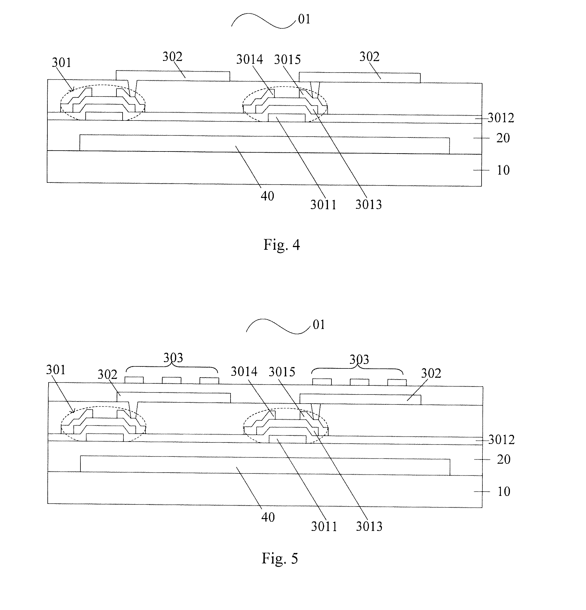
[0044]The embodiments of the present invention provide a flexible display substrate 01, as shown in FIG. 1 to FIG. 7, the flexible display substrate 01 comprises: a flexible substrate 10, a first buffer layer 20 arranged on the flexible substrate 10, a plurality of display elements 30 arranged at a side of the first buffer layer 20 away from the flexible substrate 10, each of the plurality of display elements 30 comprising a thin film transis...
PUM
 Abstract
Description
Claims
Application Information