

Method for creation of the gate shield in analog/rf power ed-cmos in sige bicmos technologies
a technology of sige bicmos and gate shields, applied in the field of misfet devices, can solve problems such as complex device fabrication
- Summary
- Abstract
- Description
- Claims
- Application Information
AI Technical Summary
Benefits of technology
Problems solved by technology
Method used
Image

Examples
third embodiment
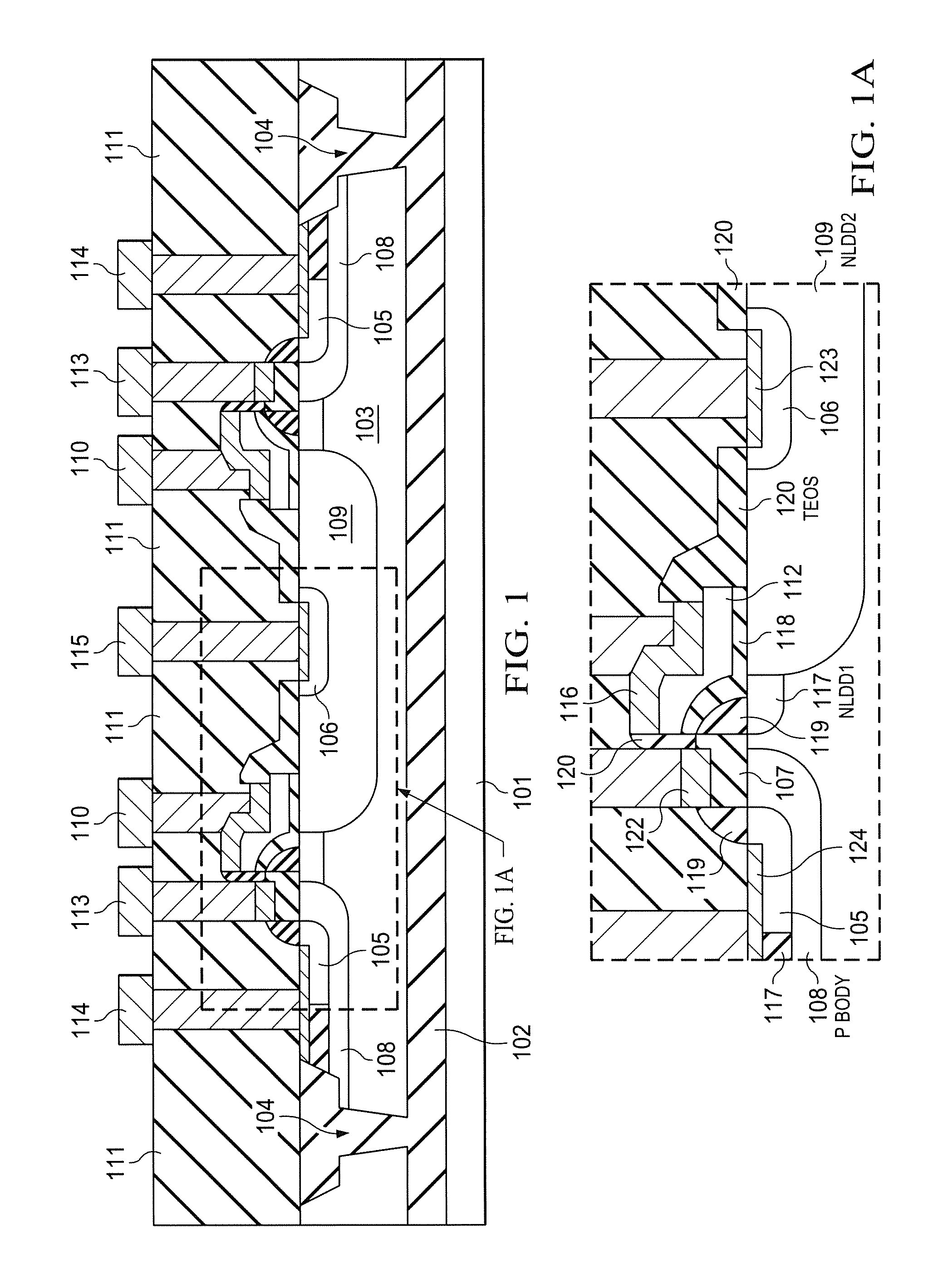
[0036]In accordance with the invention, the structure of a MOSFET transistor in a SiGe BICMOS technology will be described with reference to a laterally diffused metal oxide semiconductor LDMOS transistor, but it is to be understood that the invention is applicable to other MOSFET transistors including an extended drain MOSFET transistor, and a vertical DMOS transistor. FIG. 3 is a section view illustrating an LDMOS transistor in accordance with one embodiment of the invention and FIG. 3A is an exploded view of the shield structure of FIG. 3. In FIGS. 3 and 3A, the device includes a bulk silicon substrate 101, and an active device region 103 formed on the top surface of the bulk substrate 101, wherein deep trench isolation channels 104 define LDMOS transistor areas. Body wells 108 are formed in the active device region 103. Lateral drain wells 109 are also formed in the active device region 103, wherein the body wells 108 and the lateral drain wells 109 are spaced apart from one ano...
fourth embodiment
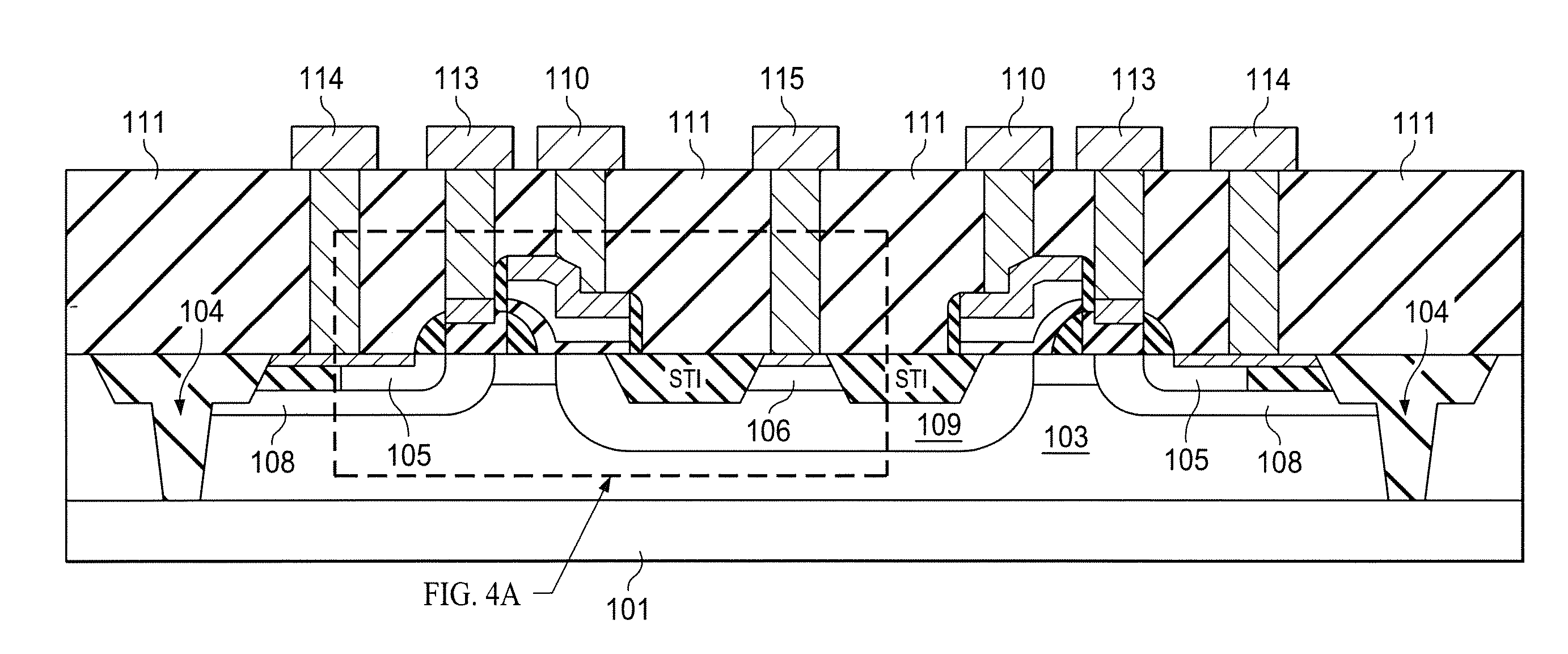
[0040]In accordance with the invention, the structure of another MOSFET transistor in a SiGe BICMOS technology will be described with reference to a laterally diffused metal oxide semiconductor LDMOS transistor, but it is to be understood that the invention is applicable to other MOSFET transistors including an extended drain MOSFET transistor, and a vertical DMOS transistor. FIG. 4 is a section view illustrating an LDMOS transistor in accordance with another embodiment of the invention and FIG. 4A is an exploded view of the shield structure of FIG. 4. In FIGS. 4 and 4A, the device includes a bulk silicon substrate 101, an active device region 103 is formed on the surface of the bulk silicon substrate 101, wherein deep trench isolation channels 104 define LDMOS transistor areas. Body wells 108 are formed in the active device region 103. Lateral drain wells 109 are also formed in the active device region 103, wherein the body wells 108 and the lateral drain wells 109 are touching one...
PUM
 Abstract
Description
Claims
Application Information