Printed wiring board

a wiring board and printed technology, applied in the direction of waveguides, waveguide type devices, high frequency circuit adaptations, etc., can solve the problems of deteriorating transmission quality, affecting the transmission quality, and the difference in transmission speed between signals that cannot be suppressed at the curved portions of signal lines, so as to achieve high transmission quality and long length

Inactive Publication Date: 2015-11-26
THE FUJIKURA CABLE WORKS LTD
View PDF13 Cites 11 Cited by
  • Summary
  • Abstract
  • Description
  • Claims
  • Application Information

AI Technical Summary

Benefits of technology

[0014]According to the present invention, in the differential signal lines, the remaining ratio of the first ground layer corresponding to the first signal line provided outside at the curved portion is lower than the remaining ratio of the second ground layer corresponding to the second signal line provided inside at the curved portion, so that the transmission speed in the first signal line having a relatively long length is relatively fast, or the transmission speed in the second signal line having a relatively short length is relatively slow. This allows input signals to be output without transmission time difference even when the lengths of a pair of signal lines that constitute differential signal lines are different. As a result, a printed wiring board having high transmission quality can be provided.

Problems solved by technology

According to the prior art, however, although the difference in propagation time caused between the signal propagating in the signal line inside at the curve and the signal propagating in the signal line outside at the curve can be compensated at the output end side, the difference in transmission speed between the signals cannot be suppressed from occurring at the curved portions of the signal lines.
This leads to a problem in that radiation noise is generated to deteriorate the transmission quality.

Method used


Image

  • Printed wiring board
  • Printed wiring board
  • Printed wiring board

Examples


first embodiment

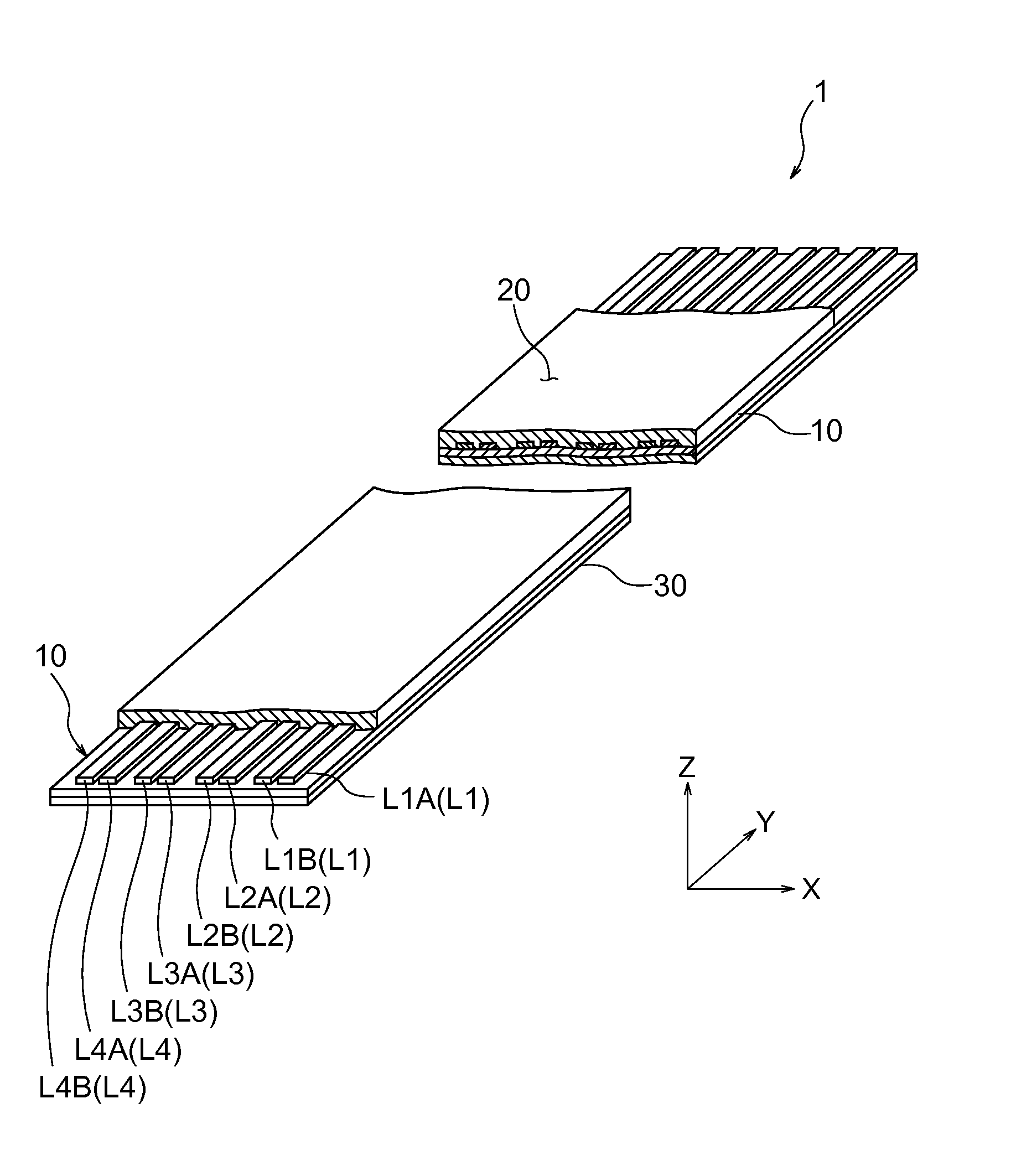
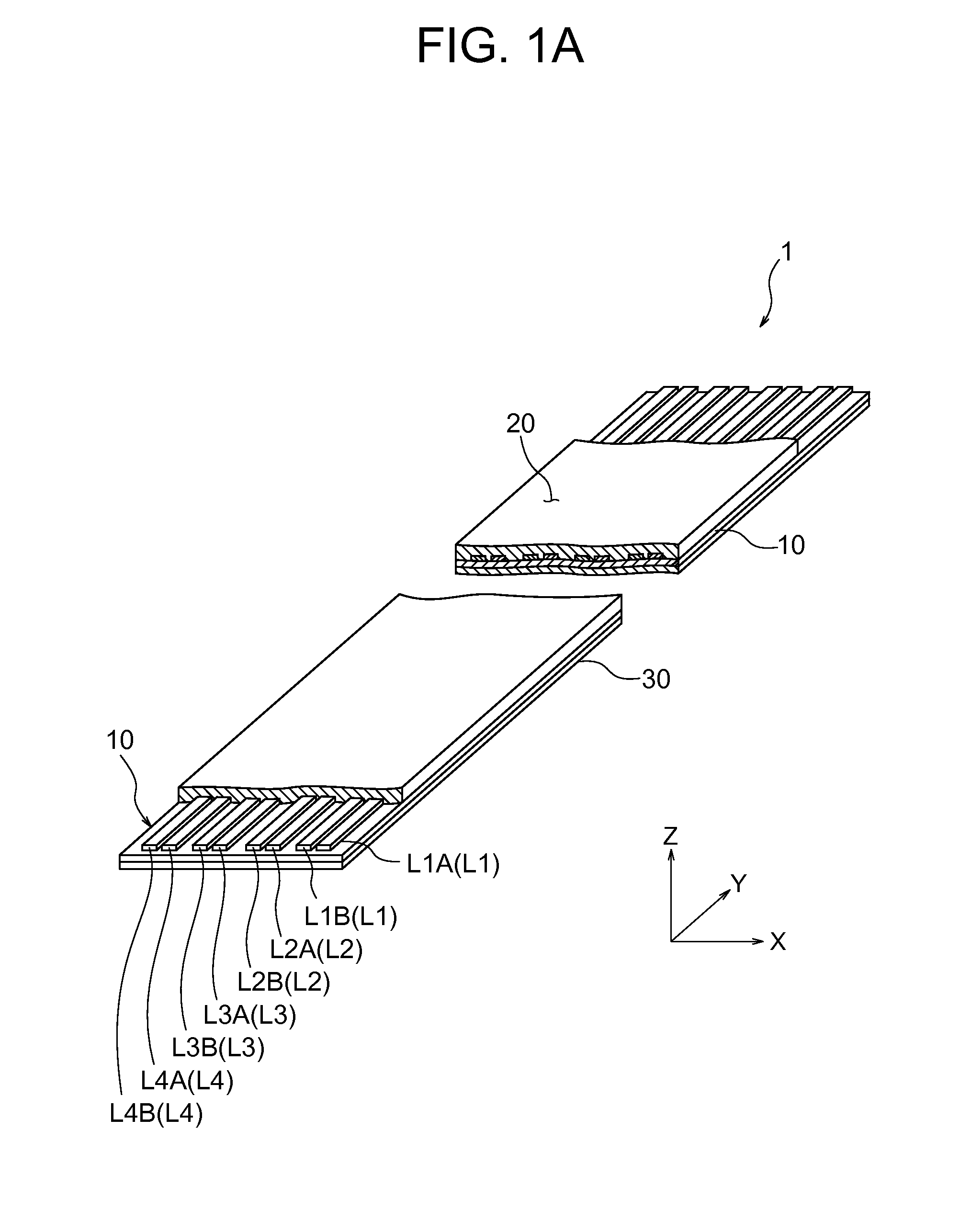
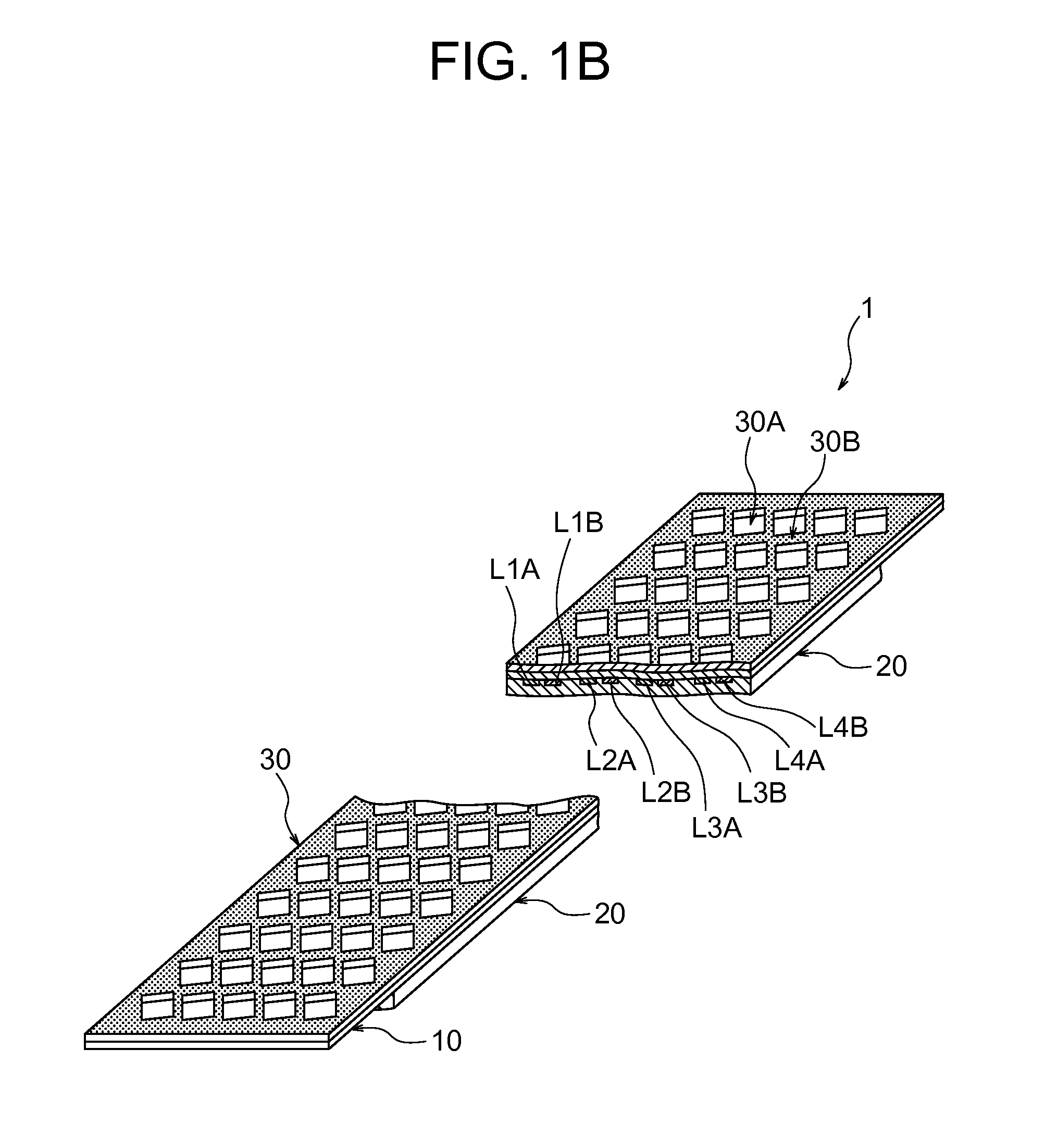
[0036]A first embodiment of the present invention will hereinafter be described with reference to the drawings. In the present embodiment, examples will be described in which a printed wiring board 1 according to the present invention may be applied to transmission lines that connect between circuits in a device, between a circuit and a device, or between devices. The printed wiring board 1 according to the present invention is suitable for transmission of high speed signals and performs differential signaling based on various standards, such as LVDS, MIPI, HDMI (registered trademark) and USB. The printed wiring board according to the present embodiment is provided with differential signal lines, which comprise at least one pair of signal lines and transmit signals in accordance with various standards to execute differential signaling. The form of the differential signal lines is not particularly limited, and a known form at the time of filing of the present application may be used ...

working example 1

[0067]A working example of a wiring board according to the present embodiment will hereinafter be described.

[0068]A copper-clad laminate was prepared such that each main surface of a polyimide substrate of a thickness of 25 mm was laminated with copper foil of a thickness of 18 μm via an adhesive of a thickness of 10 μm. Holes for through-holes were opened in the copper-clad laminate using a drill of 0.15 mm. The through-holes were formed to connect ground pads GPs (see FIG. 11A) with a lower surface ground layer (see FIG. 11A, for example). Copper plating of 15 μm was formed on the copper foil surfaces and in the through-holes. Subsequently, etching was performed using photolithography method to form signal lines L100 at the side of one main surface of the copper-clad laminate and a ground layer 30 of a mesh structure on the other main surface. Furthermore, the copper foil-exposed part was attached, in an opened state, to a cover film comprising a polyimide substrate of a thickness...

second embodiment

[0079]With reference to FIG. 7A to FIG. 10, the second embodiment will hereinafter be described. The second embodiment has a different feature that the mesh structure of the ground layer 30 is configured of a longitudinal grid pattern. Basic features and actions of the second embodiment are common with those of the first embodiment. Here, to avoid repetition in descriptions, descriptions for the common features are borrowed from those for the first embodiment.

[0080]FIG. 7A is a plan view, viewed from the side of one main surface, of an insulating substrate 10 formed with model signal lines L20 to L26 in the second embodiment. FIG. 7B is a plan view, viewed from the side of the other main surface, of the insulating substrate 10 formed with a ground layer 30 of a longitudinal grid pattern. FIG. 7C is a plan view of the insulating substrate 10 viewed from the side of the one main surface like in FIG. 7A, but with the ground layer 30 on the other main surface being transparently viewed....


PUM


Abstract

To suppress occurrence of a difference in transmission time due to a difference in length between signal lines, there is provided a printed wiring board having: an insulating substrate (10); a first signal line (L31A) that constitutes differential signal lines formed on the insulating substrate (10) and includes a curved portion; a second signal line (L31B) provided along the first signal line (L31A) and side by side inside the curved portion; and a ground layer (30) formed for the first signal line (L31A) and the second signal line (L31B) via an insulating material (10). The ground layer (30) includes a first ground layer (G31A) corresponding to a first region (D1) and a second ground layer (G31B) corresponding to a second region (D2). The first region (D1) is defined based on the first signal line (L31A) and has a first predetermined width (W31A). The second region (D2) is defined based on the second signal line (L31B) and has a second predetermined width (W31B). The first ground layer (G31A) has a remaining ratio lower than a remaining ratio of the second ground layer (G31B).

Description

BACKGROUND OF THE INVENTION[0001]1. Field of the Invention[0002]The present invention relates to a printed wiring board.[0003]2. Description of the Related Art[0004]In general, when a difference in length exists between a pair of signal lines used in differential signaling, the transmission quality deteriorates because the transmission time also differs between the signal lines.[0005]As a relevant technique, there has been known a printed wiring board in which conductor vias are formed in the vicinity of signal lines to adjust the difference in delay time of signals (Patent Document 1: JP 2011-165910 A). According to the technique described in Patent Document 1, the conductor vias are provided along straight portions of upstream side and downstream side with respect to curved portions of the signal lines thereby to delay a propagation time of a signal propagating in an inside signal line that is close to the conductor vias at the straight portions of the upstream side and the downst...

Claims


Application Information

Patent Timeline
Patent Type & Authority Applications(United States)
IPC IPC(8): H05K1/02
CPCH05K1/0237H05K1/0216H05K1/0242H05K1/0248H05K2201/093H05K2201/09263H05K2201/09236H05K2201/09681H01P3/085H05K1/0225H05K1/025H05K2201/0715H05K2201/09027H05K2201/09727H05K1/0245H05K1/0393
Inventor WATANABE, HIROHITOOGAWA, TAIJI
Owner THE FUJIKURA CABLE WORKS LTD
Why Eureka
Try Eureka