Circuit structure of liquid crystal panel and driving method of liquid crystal panel

a technology of liquid crystal display panel and circuit structure, which is applied in the direction of instruments, static indicating devices, etc., can solve the problems of increasing the resistance difference between the data driving chip and the pixels in all rows increasing the amount of output lines, and increasing the resolution of the display panel. , to achieve the effect of reducing the amount of data signal output lines of the data driving control chip and improving the color shift efficiency of the liquid crystal panel

Inactive Publication Date: 2015-12-03
TCL CHINA STAR OPTOELECTRONICS TECH CO LTD
View PDF4 Cites 4 Cited by
  • Summary
  • Abstract
  • Description
  • Claims
  • Application Information

AI Technical Summary

Benefits of technology

[0005]An objective of the present invention is to provide a circuit structure of a liquid crystal panel, the liquid crystal pixels of the M liquid crystal pixel array areas are sequentially charged without interferes with one another by sequentially triggering the M triggers. The amount of the data signal output lines of the data driving control chip is enormously reduced and the color shift of the liquid crystal panel is efficiently improved.
[0006]Another objective of the present invention is to provide a driving method of a liquid crystal panel which is capable of achieving higher resolution with a driving chip having fewer output lines. Therefore, the required manufacture cost of the driving chip in the liquid crystal panel is reduced and the color shift of the liquid crystal panel is efficiently improved.
[0034]The benefit of the present invention is: the present invention provides a circuit structure of a liquid crystal panel and a circuit structure of a liquid crystal panel. By positioning M triggers between liquid crystal pixel data signal lines and the data driving control chip, the liquid crystal panel is correspondingly divided into M liquid crystal pixel array areas. The triggers are sequentially triggered and then sequentially charging the liquid crystal pixels of the M liquid crystal pixel array areas can be achieved without interferes with one another. Charging the liquid crystal pixels of the liquid crystal panel by utilizing the n data signal output lines of the data driving control chip is realized to enormously reduce the amount of the data signal output lines of the data driving control chip and the manufacture cost of the liquid crystal panel; besides, the activation timing of the triggers is related to the dot clock signal (CLK). Therefore, the charging time of data driving control chip to the liquid crystal pixels of some liquid crystal pixel array areas become controllable. Consequently, the color shift caused by the varying charges to the left, right areas and the middle areas of the liquid crystal panel can be solved.

Problems solved by technology

However, the requirement for the amount of the output lines of the data driving control chip for the liquid crystal panel is increased accordingly and the manufacture cost gets higher along with the resolution gets higher.
However, both these two technologies requires increase of the amount of the output lines of the scan driving chip accordingly and the resistance differences from the data driving chip to the pixels in all rows of the liquid crystal panel become larger.
The color shift appears and seriously affects the image quality of the liquid crystal panel.

Method used


Image

  • Circuit structure of liquid crystal panel and driving method of liquid crystal panel
  • Circuit structure of liquid crystal panel and driving method of liquid crystal panel
  • Circuit structure of liquid crystal panel and driving method of liquid crystal panel

Examples


Embodiment Construction

[0043]Embodiments of the present invention are described in detail with the technical matters, structural features, achieved objects, and effects with reference to the accompanying drawings as follows.

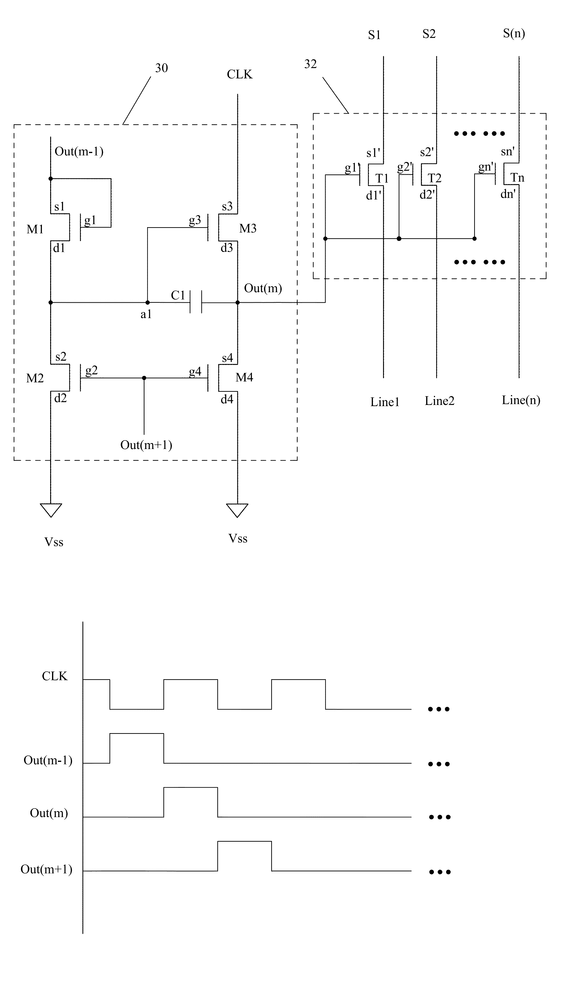
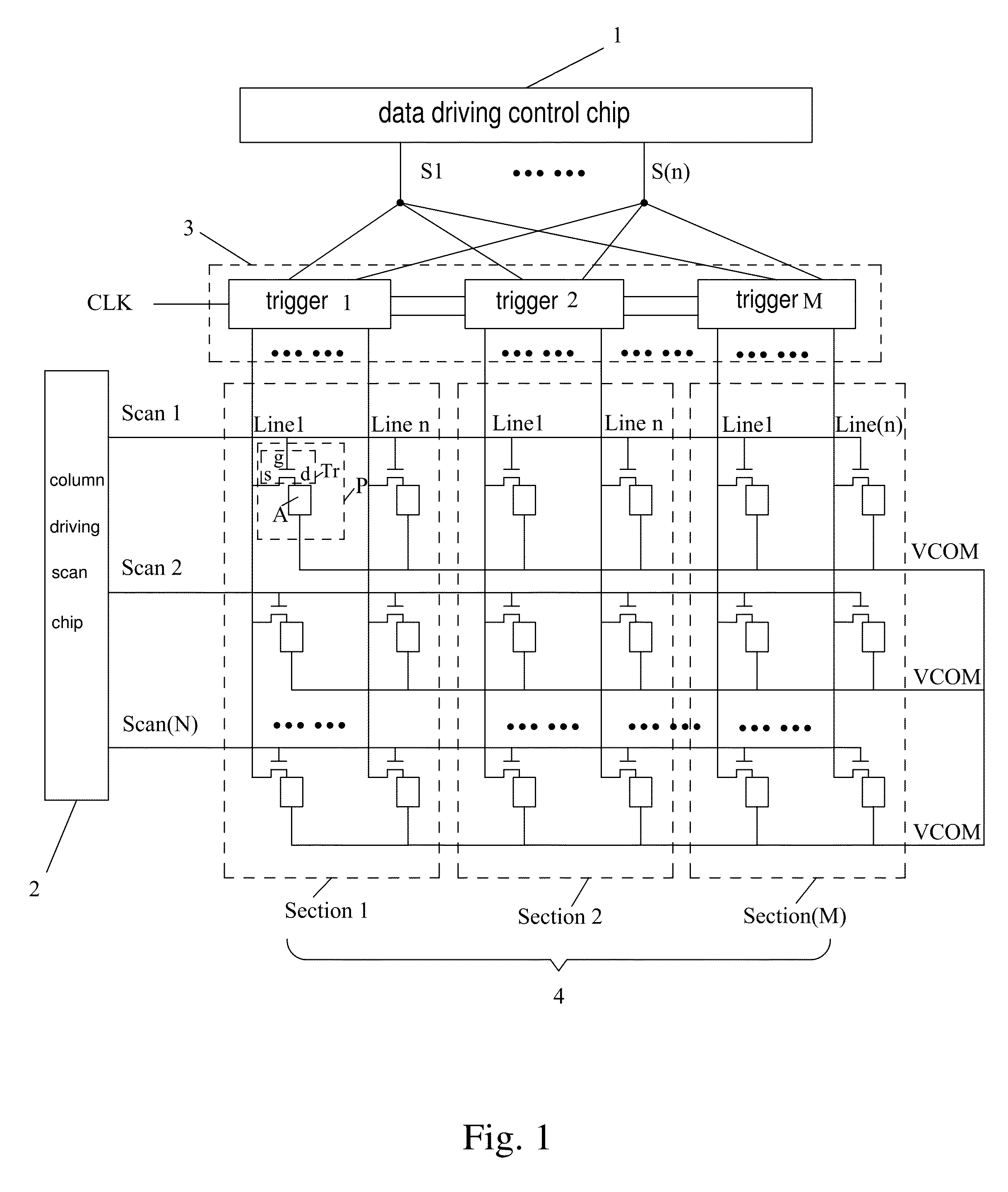
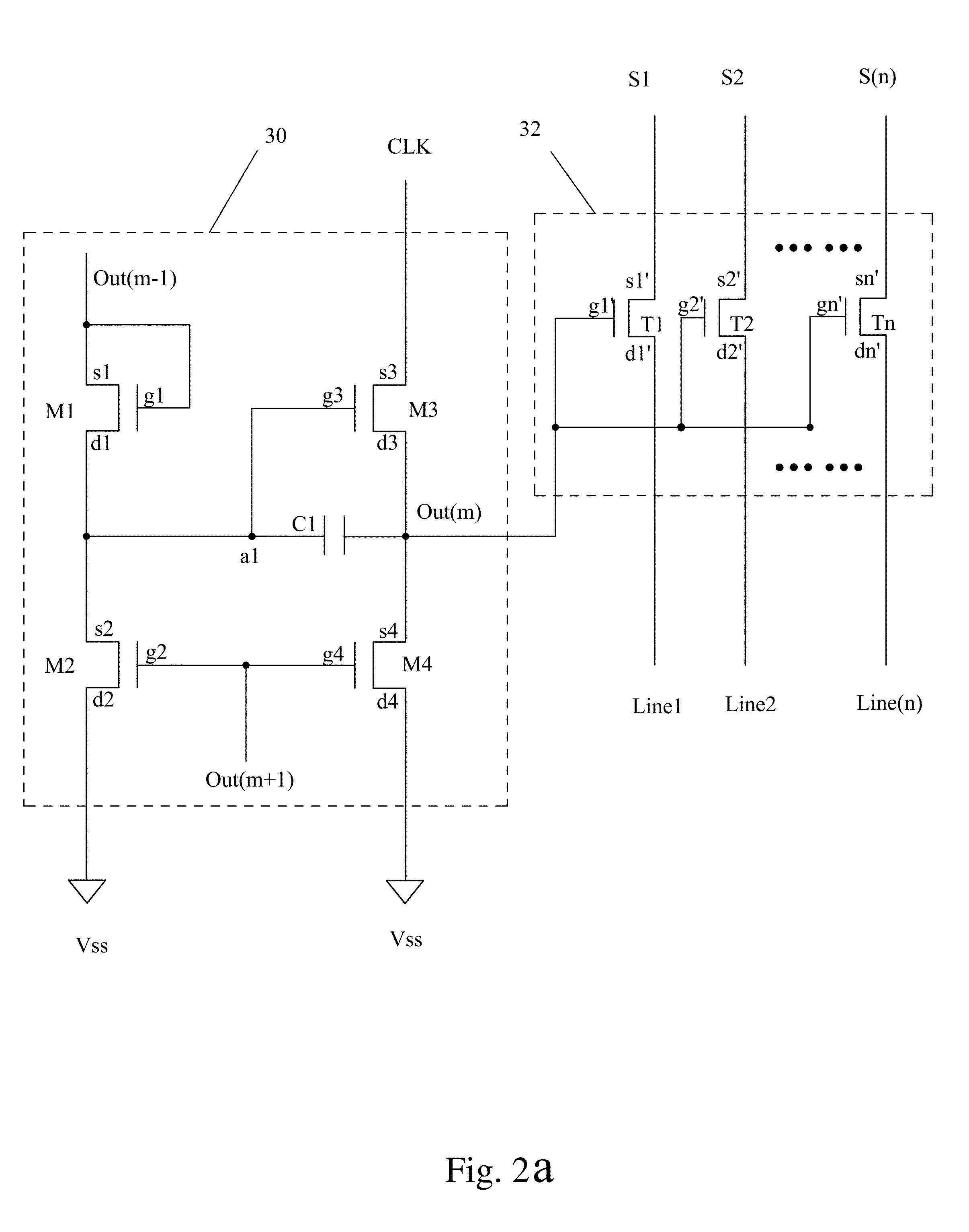
[0044]Please refer to FIG. 1. The present invention provides a circuit structure of a liquid crystal panel, comprising: a data driving control chip 1 having n data signal output lines (S1˜S(n)), a column driving scan chip 2, M triggers 3 (trigger 1˜triggerM), M liquid crystal pixel array areas 4 (Section1˜Section(M)) corresponding to the M triggers, a dot clock signal (CLK) and a common voltage (VCOM);

[0045]each of the liquid crystal pixel array areas comprises: (n×N) liquid crystal pixels (P), N scan signal lines (Scan1˜Scan(N)), and n liquid crystal pixel data signal lines (Line1˜Line(n)); n liquid crystal pixels (P) are arranged along a column direction; N liquid crystal pixels (P) are arranged along a row direction; the liquid crystal pixel (P) comprises a pixel transistor (Tr) and...


PUM


Abstract

The present invention provides a circuit structure of a liquid crystal panel and a driving method of a liquid crystal panel. The circuit structure of a liquid crystal panel comprises: a data driving control chip having n data signal output lines, a column driving scan chip, M triggers, M liquid crystal pixel array areas corresponding to the M triggers, a dot clock signal (CLK) and a common voltage (VCOM); each of the liquid crystal pixel array areas comprises: (n×N) liquid crystal pixels, N scan signal lines, and n liquid crystal pixel data signal lines; By sequentially triggering the triggers, the liquid crystal pixels of the M liquid crystal pixel array areas are sequentially charged without interferes with one another. The present invention also provides a corresponding driving method of a liquid crystal panel. The circuit structure of the liquid crystal panel and the driving method of the liquid crystal panel are capable of reducing the amount of the data signal output lines of the data driving control chip. Meanwhile, the color shift caused by the varying charges to the left, right areas and the middle areas of the liquid crystal panel can be solved.

Description

FIELD OF THE INVENTION[0001]The present invention relates to a technology field of liquid crystal display panel, and more particularly to a circuit structure of a liquid crystal panel and a driving method of a liquid crystal panel.BACKGROUND OF THE INVENTION[0002]For a common liquid crystal display, a liquid crystal layer with dielectric anisotropy is formed between the upper substrate and lower substrate. After that, the electric field density to the liquid crystal layer is controlled to change the alignment of the liquid crystal molecules. Therefore, an ideal, desired image is shown with the adjustment of the transmission light through the upper substrate, the surface of the display. The liquid crystal display comprises a liquid substrate having a plurality of pixels for showing the image, driving circuits for driving the liquid crystal panel and a back light module of projecting light to the liquid crystal panel. The equivalent circuit of each pixel composing the liquid crystal p...

Claims


Application Information

Patent Timeline
Patent Type & Authority Applications(United States)
IPC IPC(8): G09G3/36
CPCG09G3/3607G09G2320/02G09G2330/00G09G3/3688G09G2310/0297G09G2320/0242
Inventor ZHU, JIANG
Owner TCL CHINA STAR OPTOELECTRONICS TECH CO LTD
Why Eureka
Try Eureka