
Light emitting diode package structure

a technology of light-emitting diodes and package structures, which is applied in the direction of basic electric elements, electrical apparatus, and semiconductor devices, can solve the problems of unsuitable lighting devices for traditional lighting, poor heat dissipation of glues, and unpopularity in the market, and achieve better illumination efficiency and better uniformity of reflected ligh

Inactive Publication Date: 2015-12-03
CHIU SHIH YU +3
View PDF6 Cites 5 Cited by
  • Summary
  • Abstract
  • Description
  • Claims
  • Application Information

AI Technical Summary

Benefits of technology

The present invention provides a light emitting diode package structure with improved illumination efficiency, uniformity of reflected light, and full-circumference illumination angle. By separating the light emitting diode chip and the encapsulation case, the surface of the chip is not directly covered by a colloid, resulting in improved illumination efficiency and uniformity of reflected light. The phosphor layer coated on the encapsulation case and the separate distance between the chip and encapsulation case provide full-circumference illumination angle, making it suitable for replacing traditional light devices without noticeable differences.

Problems solved by technology

Therefore, the LED lighting module designed according to the aforementioned features faces the drawbacks of limited illumination angle, single directional light source, and different illumination property as the traditional lighting source, which make the LED unsuitable for being used in the traditional lighting device.
Therefore, except being able to replace the halogens light used as jewelry Lighting, and the MR16 lighting device used in display windows, the LED is not yet popular in the market due to the disadvantages of limited illumination angle and high price of LED lighting.
However, the glue is not good in heat dissipation, and the LED will generate heat when in operation.
The heat will decrease the working efficiency and the life of the LED, and the glue accumulates the heat.
Moreover, the glue can further restrict the illumination angle, which results in the features of the LED after packaging: directivity, surface light source.
Therefore, when using in some traditional lighting device, the illumination effect of LED cannot create the same comfort feeling as the traditional light source.
However, the cost of this electrophoresis coating technology disclosed in this patent is very expensive, which cannot reduce the cost of the LED, and thus the LED manufactured by this method does not have the price advantage.
Besides, in the method which attaches phosphor coated sheet onto the LED, the phosphor coated sheet needs to be prepared separately, resulting complicated manufacturing process.
In addition, the process attaching the phosphor coated sheet needs to be very precise, and the yield is not easy to control, thereby increasing the cost of the manufacturing process.
However, this approach is not able to solve the directivity problem of the conventional light emitting diode package.
However, the encapsulating glue is still attached to the entire light-emitting diode, which also results in heat dissipating problem and lacks reliability.

Method used


Image

  • Light emitting diode package structure
  • Light emitting diode package structure
  • Light emitting diode package structure

Examples


Embodiment Construction

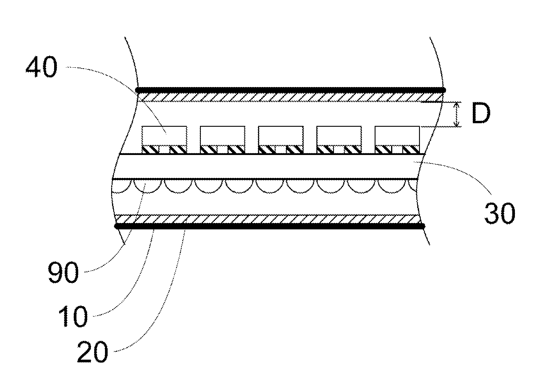
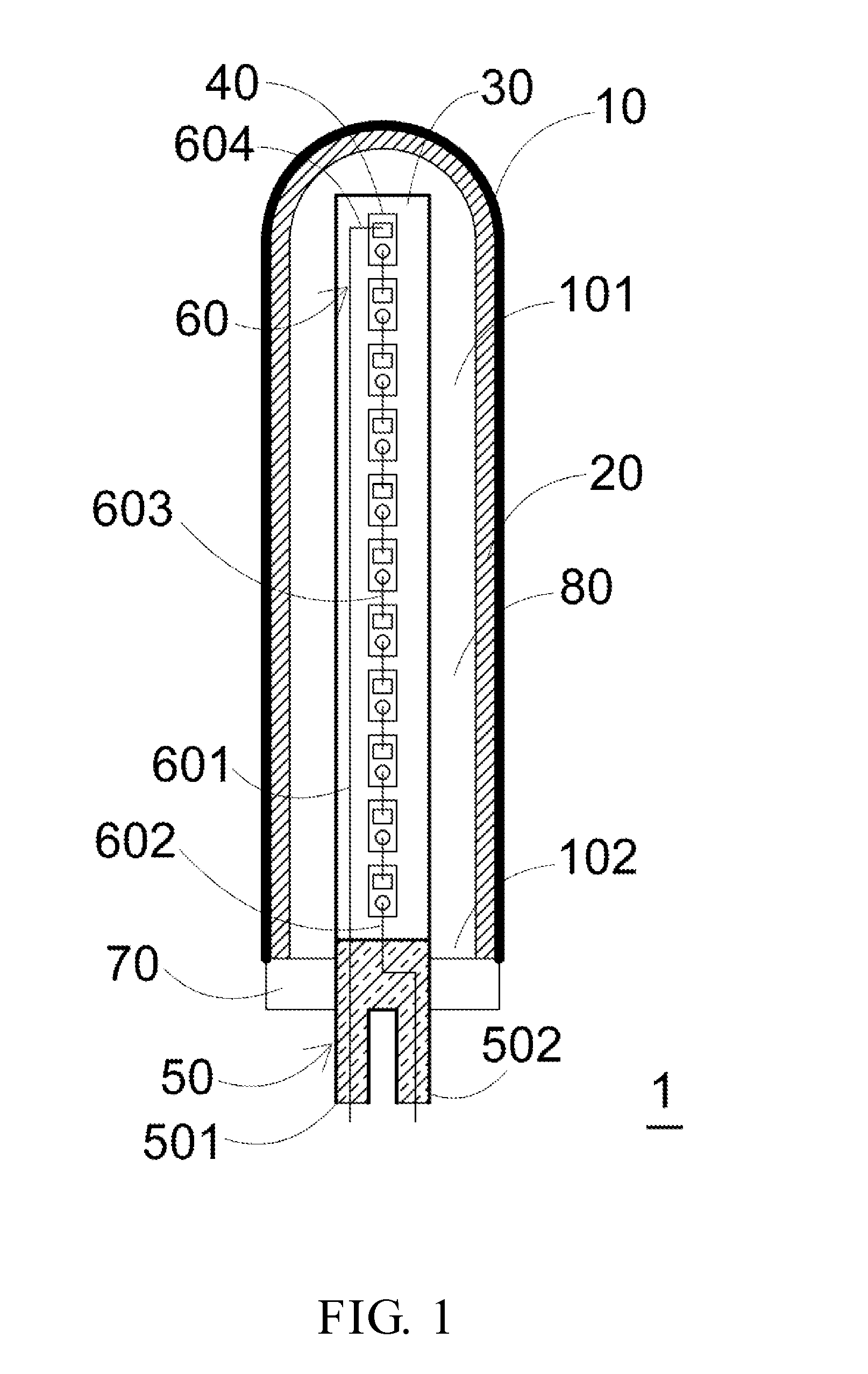
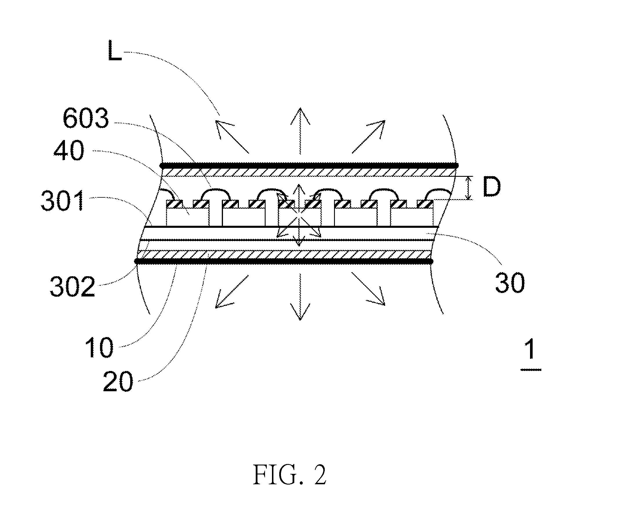
[0041]Please refer to FIGS. 1 and 2, in the preferred embodiment of the present invention, the light emitting diode package structure 1 includes an encapsulation case 10, a phosphor layer 20, a substrate 30, and a light emitting diode chip 40. The encapsulation case 10 has an accommodating space 101. The phosphor layer 20 is coated on a side of the encapsulation case 10. The substrate 30 is disposed inside the accommodating space 101. The light emitting diode chip 40 is disposed on a first surface 301 of the substrate 30 and is separated from the phosphor layer 20 by a distance D.

[0042]Specifically, in the preferred embodiment of the present invention, a material of the encapsulation case 10 is selected from a group consisting of poly methyl methacrylate, polycarbonate, SiO2, BK7, and glass. The encapsulation case 10 includes an opening 102. The substrate 30 is disposed inside the accommodating space 101 through the opening 102.

[0043]In the preferred embodiment of the present invent...


PUM


Abstract

A light emitting diode package structure includes an encapsulation case, a phosphor layer, a substrate, and a light emitting diode chip. The encapsulation case has an accommodating space. The phosphor layer is coated on a side of the encapsulation case. The substrate is disposed in the accommodating space. The light emitting diode chip is disposed on a first surface of the substrate. A surface of the light emitting diode chip is devoid of being directly covered by a colloid, and the light emitting diode chip and the package housing are separated from each other by a distance.

Description

TECHNICAL FIELD [0001]The technical field relates to a light emitting diode package structure, particularly to a full-circumference light emitting diode package structure.RELATED ART [0002]Since Dr. Shuji Nakamura from Nichia of Japan successes in epitaxial growth on a sapphire substrate GaN material to produce the first mass producible blue light-emitting diode (blue LED) in 1995, complements for the previously available red and green only LED is completed, making the LED to be formally changed to full-color LED. After white LED is developed by mixed light package of the InGaN blue LED and the phosphor powder in 1996, a variety of LED applications are revealed, which introduces LED into human life, and this white LED package so far is still one of the mainstream technologies.[0003]The main purpose of the LED package is to protect the LED, preventing moisture and the touching when in use. By the superior stent cooling structure, the reliability and service life of LED products can b...

Claims


Application Information

Patent Timeline
IPC IPC(8): H01L33/54H01L33/62H01L33/44H01L33/50H01L33/24H01L33/36H01L27/15H01L33/56H01L33/04
CPCH01L33/54H01L33/56H01L33/62H01L33/44H01L33/502H01L33/24H01L33/36H01L27/15H01L33/04H01L25/0753H01L33/48H01L33/507H01L33/508H01L33/52H01L2224/48091H01L2224/48137H01L2224/45144H01L2924/00014H01L2924/00
Inventor CHIU, SHIH-YU
Owner CHIU SHIH YU
Learn More