P-doping of group-iii-nitride buffer layer structure on a heterosubstrate

a heterosubstrat and buffer layer technology, applied in the direction of semiconductors, electrical devices, transistors, etc., can solve the problems of undesired parasitic conductive channels in the buffer layer structure, and achieve the effects of reducing the concentration of p-type dopants, improving crystal quality, and improving the flow rate of gallium precursors

Active Publication Date: 2015-12-10
AZUR SPACE SOLAR POWER
View PDF1 Cites 22 Cited by
  • Summary
  • Abstract
  • Description
  • Claims
  • Application Information

AI Technical Summary

Benefits of technology

[0013]The buffer layer structure of the invention can be based on the recognition, that group-III nitrides grown on a heterosubstrate are subjected to substantial stress during the manufacturing process. In comparison with a deposition on a homosubstrate, this requires a special stress management in the buffer-layer structure. One stress management measure is including in the buffer layer structure a stress management layer sequence of an interlayer structure that is arranged between and adjacent to a first group-III-nitride layer and a second group-III-nitride layer, which have a smaller band gap than a group-III-nitride interlayer material. However, the provision of this stress management layer sequence implies the risk of a formation of undesired parasitic conductive channels in the buffer layer structure. The invention is based on the further recognition that an incorporation of carbon or magnesium as p-type dopant in the stress management layer sequence with a suitable concentration profile across the stress management layer sequence is effective in avoiding the formation of such parasitic conductive channels in the buffer layer structure. This way, it becomes even possible in some embodiments to avoid any intentional incorporation of iron atoms, which, as described, have been used in the prior art to achieve a highly resistive buffer layer structure.
[0044]In an embodiment of the method before the deposition of the stress management layer sequence a AlN nucleation layer is deposited on the substrate by a vapor phase deposition technique using a hydrogen-free carrier gas, preferably N2, at a temperature between 800 and 1030° C., followed by a deposition of a buffer stack before depositing the stress management layer sequence by using Tetraethylgallium and Trimethylaluminum as precursors at a temperature between 800 and 1030° C., wherein the buffer stack comprises either a compositionally graded AlGaN buffer layer having a Ga fraction increasing with increasing distance from the heterosubstrate, or a superlattice formed by a stack of alternating group-III-nitride layers of two kinds. The low temperatures during the growth of the AlN nucleation layer and the buffer stack are advantageous for the incorporation of carbon concentrations of more than 1×1017 cm−3 and lead to a better crystal quality.

Problems solved by technology

However, the provision of this stress management layer sequence implies the risk of a formation of undesired parasitic conductive channels in the buffer layer structure.

Method used


Image

  • P-doping of group-iii-nitride buffer layer structure on a heterosubstrate
  • P-doping of group-iii-nitride buffer layer structure on a heterosubstrate
  • P-doping of group-iii-nitride buffer layer structure on a heterosubstrate

Examples


Embodiment Construction

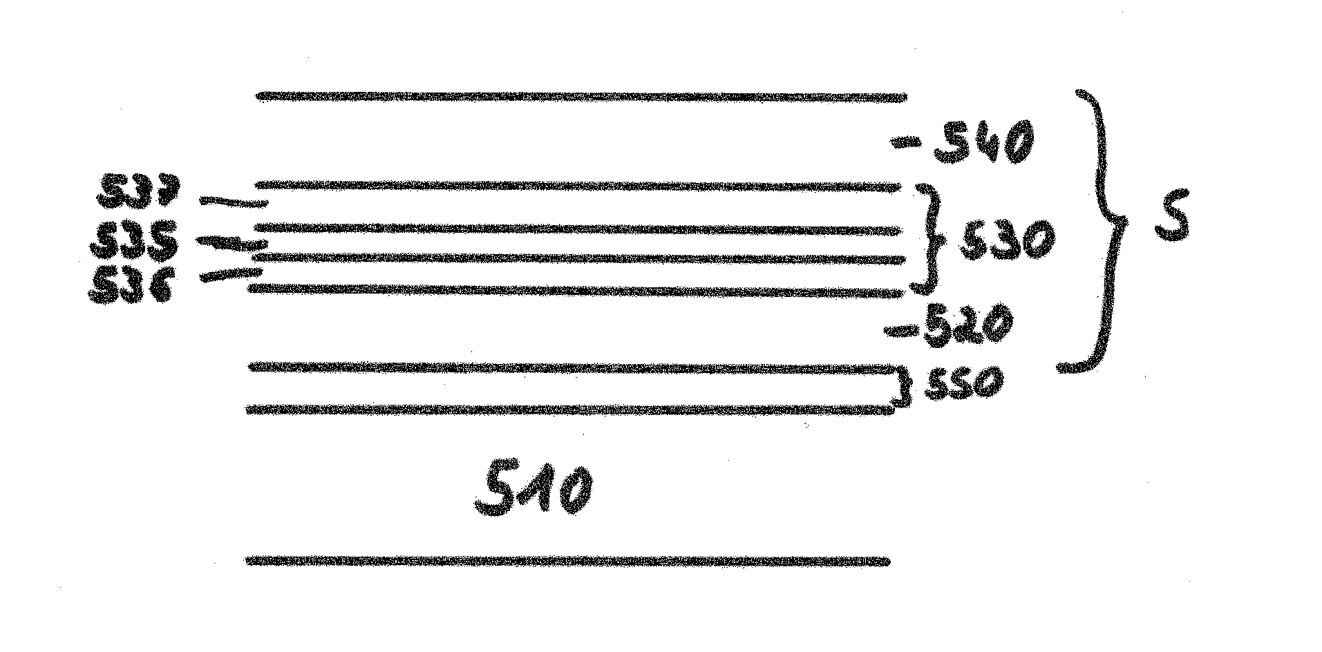
[0057]FIG. 1 shows an embodiment of a buffer layer structure 100 according to the invention. On a substrate 110, which in the present embodiment is made of silicon or silicon carbide, an intermediate layer may be grown. This intermediate layer is not shown in detail in FIG. 1, but only indicated by a space above the substrate 110. Such intermediate layer, which may contain a sub-layer structure, serves for achieving nucleation and initial lattice adaptation. In some embodiments, however, the intermediate layer may be omitted, and the buffer layer structure grown directly on the substrate. Examples of an intermediate layer in the form of a buffer stack will be described further below.

[0058]The buffer layer structure 100 comprises a stress management layer sequence S. The stress management layer sequence is formed of three group-III-nitride layers 120 to 140, of which a single interlayer 130 is sandwiched between a first group-III-nitride layer 120 and a second group-III-nitride layer...


PUM


Abstract

An epitaxial group-ill-nitride buffer-layer structure is provided on a heterosubstrate, wherein the buffer-layer structure has at least one stress-management layer sequence including an interlayer structure arranged between and adjacent to a first and a second group-ill-nitride layer, wherein the interlayer structure comprises a group-ill-nitride interlayer material having a larger band gap than the materials of the first and second group-ill-nitride layers, and wherein a p-type-dopant-concentration profile drops, starting from at least 1×1018 cm-3, by at least a factor of two in transition from the interlayer structure to the first and second group-ill-nitride layers.

Description

[0001]This nonprovisional application is a continuation of International Application No. PCT / EP2014 / 052957, filed on Feb. 14, 2014, which claims priority to European Patent Application No. 13155540.1, filed on Feb. 15, 2013, both of which are herein incorporated by reference.BACKGROUND OF THE INVENTION[0002]1. Field of the Invention[0003]The present invention relates to an epitaxial group-III-nitride buffer layer structure on a heterosubstrate. It also relates to a device structure, in particular to a layer structure of a transistor, a field-effect transistor (FET), a high-electron-mobility transistor (HEMT), in particular a normally-on or normally-off HEMT or a metal-insulator-semiconductor (MIS)HEMT, a Schottky diode, or a P-I-N structure.[0004]2. Description of the Background Art[0005]Most group-III-nitride based device structures, in particular transistor structures used nowadays for radio frequency (RF) or high-voltage (HV) power-conversion devices, are fabricated on a heterosu...

Claims


Application Information

Patent Timeline
Patent Type & Authority Applications(United States)
IPC IPC(8): H01L29/205H01L29/778H01L21/02H01L33/00H01L29/15H01L29/36H01L29/872
CPCH01L29/205H01L29/36H01L29/778H01L21/0254H01L33/0025H01L29/151H01L29/872H01L21/02378H01L21/02381H01L21/02458H01L21/02505H01L21/02507H01L21/0251H01L21/02579H01L29/7783H01L29/1075H01L29/2003H01L29/207
Inventor LUTGEN, STEPHANMURAD, SAADCHITNIS, ASHAY
Owner AZUR SPACE SOLAR POWER
Why Eureka
Try Eureka