Wafer Leveled Chip Packaging Structure and Method Thereof
a chip and packaging technology, applied in the direction of electrical equipment, semiconductor devices, semiconductor/solid-state device details, etc., can solve the problems of large dip, large mounting area, insufficient dip, etc., to reduce fabrication costs and increase mass production yield
- Summary
- Abstract
- Description
- Claims
- Application Information
AI Technical Summary
Benefits of technology
Problems solved by technology
Method used
Image

Examples
embodiment 1
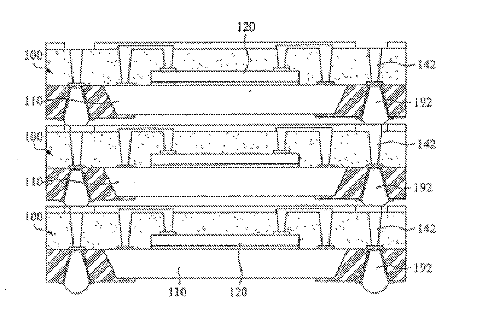
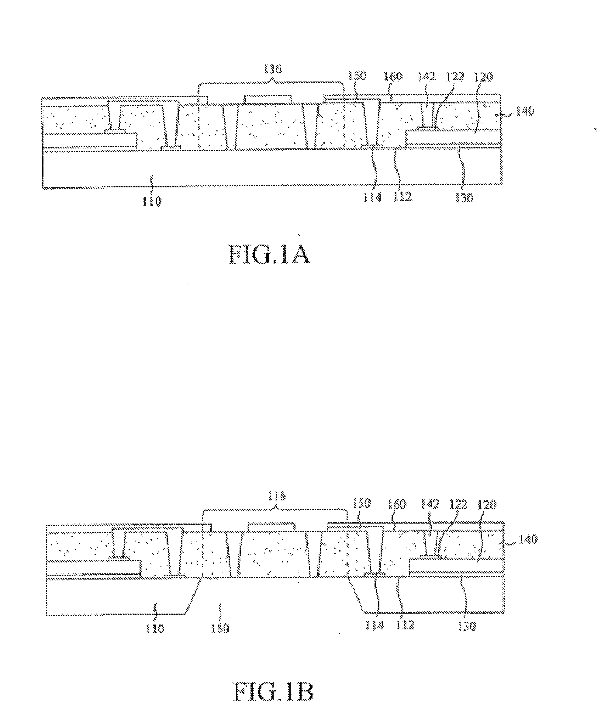
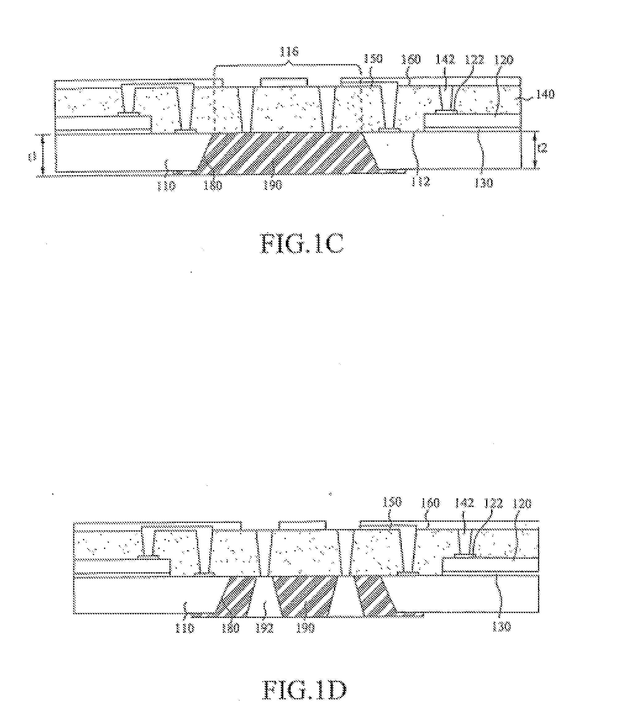
[0029]A wafer-leveled chip packaging method of this embodiment comprises the following steps. First, referring to FIG. 1A, a silicon wafer 110 having an integrated circuit is provided. The silicon wafer 110 has a first surface 112 on which a plurality of pads 114 is mounted. Then, a plurality of first chips 120 each having at least one pad 122 is attached to the first surface 112 of the silicon wafer 110 with an adhesive 130, wherein the pad 122 is disposed on a surface opposed to the silicon wafer 110. Then, a first insulating layer 140 is laminated on the first surface 112 of the silicon wafer 110. Next, a plurality of via-holes is formed by laser or photolithography, and after that a conducting material is filled in the via-holes by electroplating, electroless plating or the combination thereof so as to form a plurality of first conductive vias 142 penetrating the first insulating layer 140. Parts of first conductive vias 142 are connected with the pads 114 of the silicon wafer 1...
embodiment 2
[0035]Referring now to FIG. 3, the second embodiment of a wafer-leveled chip packaging method of the present invention is disclosed, which comprises the following steps. A silicon wafer 110 having an integrated circuit pattern is provided. The silicon wafer 110 has a first surface 112 on which a plurality of pads 114 is mounted. Then, a plurality of first chips 120 each having at least one pad 122 is attached to the first surface 112 of the silicon wafer 110 with a non-conductive adhesive 130, wherein the pad 122 is disposed on a surface opposed to the silicon wafer 110, whereafter a first insulating layer 140 is coated on the first surface 112 of the silicon wafer 110. Then, a plurality of via-holes is formed by laser drilling.
[0036]Next, a conducting material is filled in the via-holes by electroplating or electroless plating so as to form a plurality of first conductive vias 142 penetrating the first insulating layer 140. Parts of first conductive vias 142 are connected with the ...
embodiment 3
[0038]Referring to FIG. 4, this embodiment discloses a wafer-leveled chip packaging method comprising following steps. A silicon wafer 110 having a first surface 112 is provided. An insulating layer 220 and a second conductive pattern layer 230 are formed sequentially on the first surface 112 of the silicon wafer 110. Then, an anisotropic conductive glue 240 is used to bond a first chip 120 to the silicon wafer 110 with the surface having a circuit pattern formed thereon for additional heat transferring, wherein the second conductive pattern layer 230 formed on the silicon wafer 110 is electrically connected with the first chip 120. A first insulating layer 140 is laminated on the silicon wafer 110. Then, a plurality of via-holes is formed by photolithography and a conducting material is filled in the via-holes by electroless plating to form a plurality of first conductive vias 142 which pass through the first insulating layer 140. Parts of the first conductive vias 142 are connecte...
PUM
 Abstract
Description
Claims
Application Information
 - R&D
- Intellectual Property
- Life Sciences
- Materials
- Tech Scout
- Unparalleled Data Quality
- Higher Quality Content
- 60% Fewer Hallucinations
Browse by: Latest US Patents, China's latest patents, Technical Efficacy Thesaurus, Application Domain, Technology Topic, Popular Technical Reports.
© 2025 PatSnap. All rights reserved.Legal|Privacy policy|Modern Slavery Act Transparency Statement|Sitemap|About US| Contact US: help@patsnap.com