Scintillation Detector

a detector and detector technology, applied in the field of scintillation detectors, can solve the problems of low image contrast, additional reduction of contrast, complex existing technology used for establishing pixellated elements within phosphor coatings, etc., and achieve the effect of reducing scattering effect and increasing separation properties

Inactive Publication Date: 2015-12-31
STC MT
View PDF0 Cites 8 Cited by
  • Summary
  • Abstract
  • Description
  • Claims
  • Application Information

AI Technical Summary

Benefits of technology

[0014]The essential difference of the proposed scintillation detector is the new design concept presented in the form of a structured array of mutually isolated elements formed on the surface of the photosensitive area of photosensor cells. The localized and isolated arrangement of each scintillator element (relative to the other elements) provides their optical separation at the scintillator layer level, which avoids the noise light quantum illumination and scattering between neighboring cells of the photosensor cells, i.e. it eliminates scattering effect between bordering cells, thereby it allows to achieve the claimed technical result. The separation properties can be increased by wave-guiding features of the scintillator elements.

Problems solved by technology

The disadvantage of the mentioned scintillation detector is the low contrast of the image due to optical scattering in phosphor neighboring elements.
Also, internal reflections may occur in the lower layer, what would lead to additional reduction of the contrast.
Complexity of its technology represents an additional disadvantage of this structure: firstly, the need to align the groove grid relative to the matrix of photosensitive cells; secondly, the complexity of existing technologies used for establishing of pixellated elements within phosphor coatings.

Method used


Image

  • Scintillation Detector
  • Scintillation Detector
  • Scintillation Detector

Examples


Embodiment Construction

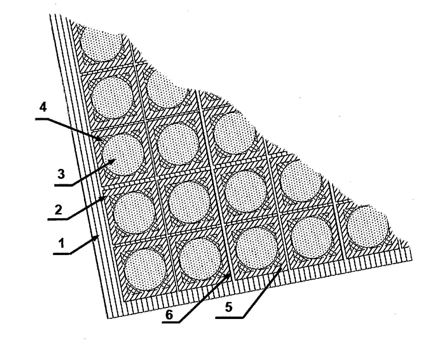
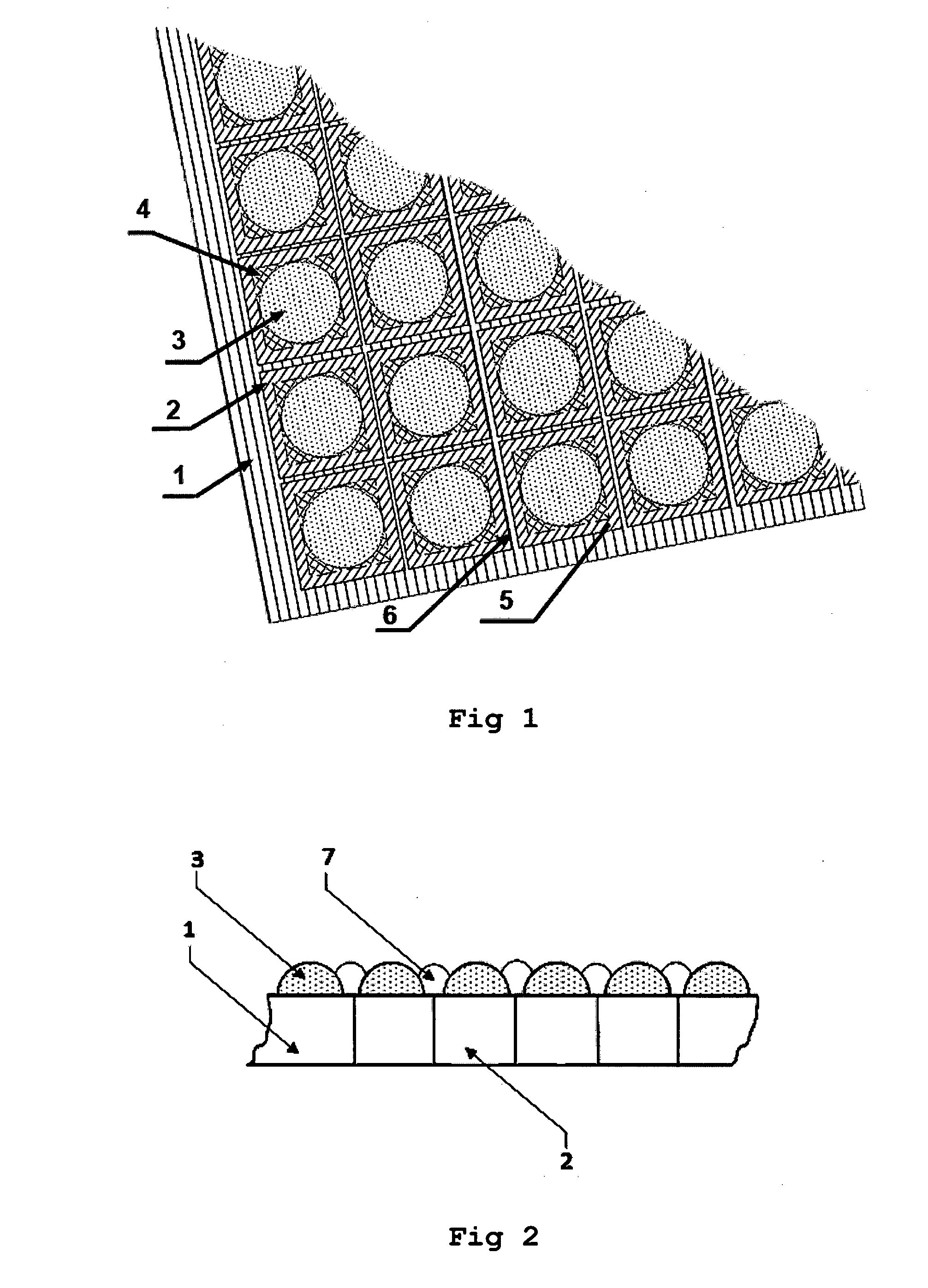
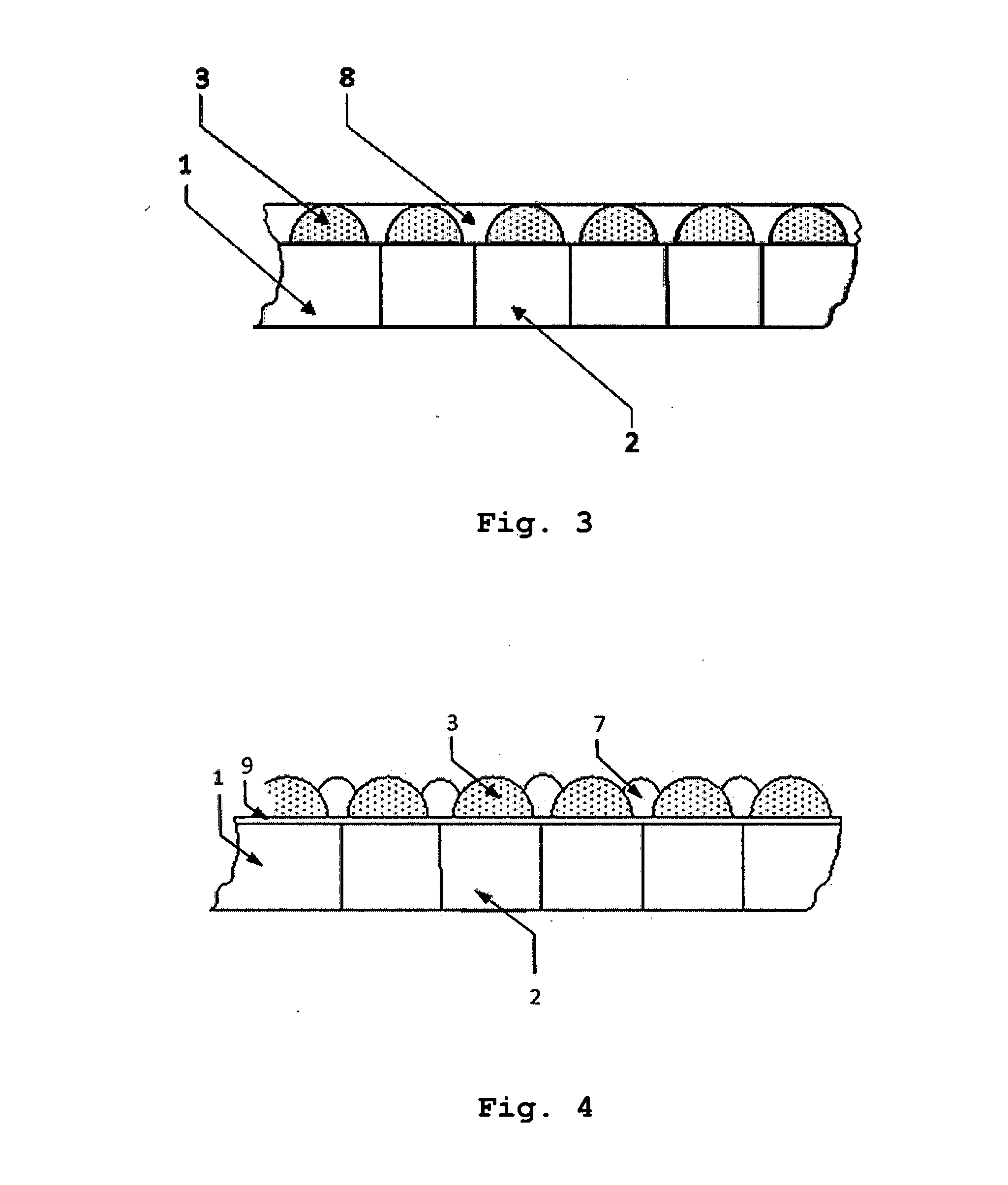
[0019]FIG. 1 shows a scintillation detector with at least one photosensor 1 with a matrix of cells 2 and an array of structured scintillators with mutually isolated elements 3. Each of the cells 2 has photosensitive zone 4 and a zone 5 of low sensitivity (or insensitive zone). The electrical contacts 6 are located between the cells and these contacts are sealed with transparent dielectric (not shown). Normally the sensitive area of zone 4 has a much more large area than the zone of low sensitivity 5.

[0020]Scintillator elements 3 formed on the surface of the photosensor 1 are made using at least one nano-composite based on a phosphor with corresponding range of the detected radiation, e.g., X-rays or gamma radiation. As a nano-composite, one can use any known nano-particle phosphors-based material with efficient registration of the target radiation.

[0021]Location of the scintillation elements 3 spatially correlated with cell-matrix 2 of the photosensor 1, wherein each scintillator el...


PUM


Abstract

The invention relates to X-ray imaging devices, particularly to devices for X-ray mammography and tomosynthesis. The scintillation detector comprises at least one photosensor with an array of cells each of thereof has a photosensitive area, and a scintillator arranged in the form of a structured aggregate made of elements isolated from each other and placed on the surface of the photosensor. The new construction of the proposed scintillation detector is the completely eliminated need for precise alignment of the structured scintillator based on the elements with a matrix of cells of a photosensor. Precise arrangement of the scintillation elements and the matrix of cells of a photosensor is performed directly during the formation of the scintillation elements. The technical result achieved by using the invention is the increase of image contrast.

Description

TECHNICAL FIELD OF THE INVENTION[0001]The invention relates to the devices intended for obtaining X-ray or gamma radiation images, in particular to the devices for X-ray mammography, tomosynthesis and Non Destructive Testing systems.PRIOR ART[0002]So-called “Flat panel” visible image detectors (photosensors) are conventionally used for constructing the digital x-ray detectors including mammographic detectors, which detect the visible light field converted from the X-ray shadow image of the object. Such flat panel detectors are full-scale 2D matrix image sensors with 1:1 scale transformation.[0003]The photosensor itself has a high sensitivity at the wavelength bandwidth of visible light (400-700 nm) and is usually not sensitive to X-ray radiation. Thus the X-ray image is to be converted into visible light, and scintillating screens (scintillators) are used for that. Scintillator screens are based on the phosphor layers of specified efficiency and scattering characteristics. This scre...

Claims


Application Information

Patent Timeline
Patent Type & Authority Applications(United States)
IPC IPC(8): G01T1/20
CPCG01T1/2002G01T1/20
Inventor SUPONNIKOV, DMITRIY ALEKSANDROVICHPUTILIN, ANDREY NIKOLAEVICHDABAGOV, ANATOLY RUDOLFOVICH
Owner STC MT
Why Eureka
Try Eureka