IC layout adjustment method and tool for improving dielectric reliability at interconnects

a dielectric reliability and layout adjustment technology, applied in the field of integrated circuit and integrated circuit fabrication, can solve the problems of the limitations of modern lithography techniques and inherent variation in processing capabilities, and the inability to meet the requirements of sub-wavelength lithography, so as to avoid rejection by a design rule checker

Active Publication Date: 2015-12-31
RGT UNIV OF CALIFORNIA
View PDF3 Cites 20 Cited by
  • Summary
  • Abstract
  • Description
  • Claims
  • Application Information

AI Technical Summary

Benefits of technology

[0018]A preferred method is a method for adjusting a layout used in making an integrated circuit. One or more interconnects in the layout that are susceptible to dielectric breakdown are selected. One or more selected interconnects are adjusted to increase via to wire spacing with respect to at least one via and one wire of the one or more selected interconnects. Layout adjustments including changes made by said moving are provided. Preferably, the selecting analyzes signal patterns of interconnects, and estimates the stress ratio based on state probability of routed signal nets in the layout. In preferred embodiments, tan annotated layout is provided that describes distances by which one or more via or wire segment edges are to be shifted. In a preferred embodiment, an optical proximity correction solution is provided that contains at least one shifted via or wire edge as a layout adjustment. IC manufacturing proceeds with a adjusted layout. With an annotated layout, rejection by a design rule checker can be avoided, though the adjusted layout may violate a design rule if presented to the DRC. Adjustments can include thinning and shifting of wire segments, and rotation of vias.

Problems solved by technology

Sub-wavelength lithography presents many challenges to manufacturers trying to maintain the economic scaling of semiconductors postulated by Moore's Law.
The limits of modern lithography techniques and inherent variation in processing capabilities often create misalignments between vias and wires.
While this permits reducing node size, it increases the risk of via misalignment during manufacture.
An undesirable conducting path forms between interconnects adjacent interconnects when dielectric breakdown occurs.
Photomask misalignment between via and wire has been recognized as a cause of smaller via-to-wire spacing, and degraded time-dependent dielectric breakdown reliability.
The impact of layout adjustment on time-dependent dielectric breakdown is unaccounted for in the adjustment, however, and may produce poor time-dependent dielectric breakdown reliability.
While time-dependent dielectric breakdown reliability has been studied and characterized, time-dependent dielectric breakdown remains a major reliability issue for advanced integrated circuit technology, especially with the push to achieve reliability with sub 45 nm nodes. spacing and voltage trends projected by the International Technology Roadmap for Semiconductors (ITRS) lead to an increasing electric field as technology scales.
Moreover, the via-to-wire misalignment is expected to worsen in advanced technology when the vias must land on wires that are misaligned due to litho-etch-litho-etch double-patterning Such a worsening time-dependent dielectric breakdown reliability trend will limit wiring pitch and / or the maximum allowed supply voltage.

Method used


Image

  • IC layout adjustment method and tool for improving dielectric reliability at interconnects
  • IC layout adjustment method and tool for improving dielectric reliability at interconnects
  • IC layout adjustment method and tool for improving dielectric reliability at interconnects

Examples


Embodiment Construction

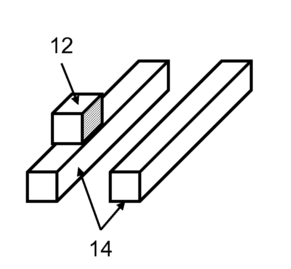
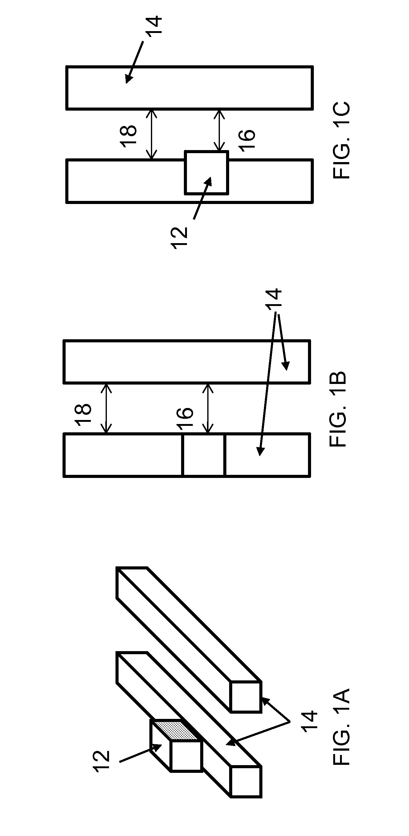
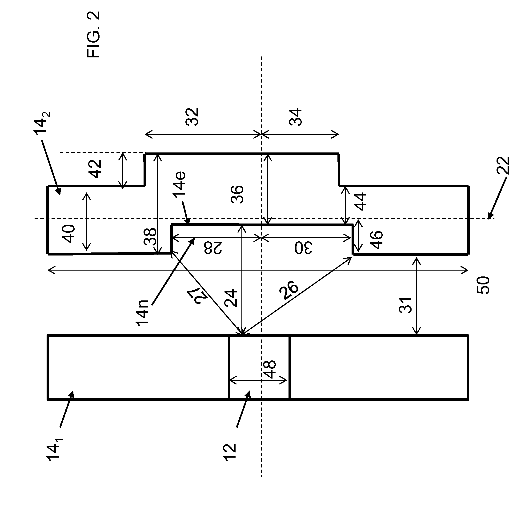
[0036]The invention provides systems and methods for adjusting a layout used in making an integrated circuit. One or more interconnects in the layout that are susceptible to dielectric breakdown are selected. One or more selected interconnects are adjusted to increase via to wire spacing with respect to at least one via and one wire of the one or more selected interconnects. The adjusted layout is used to manufacture an IC. The layout can be used by a lithography system. Layout adjustments including changes made by said moving are provided. In a preferred method the providing creates annotated layout that defines one or more geometry adjustments to be performed on the one or more selected interconnects. In another preferred method, the providing comprises creates a adjusted layout that defines the pattern for the one or more selected interconnects. Preferred embodiments are implemented in optical proximity correction tool. Selected interconnect can include a square or rectangular vi...


PUM


Abstract

Method for adjusting a layout used in making an integrated circuit includes one or more interconnects in the layout that are susceptible to dielectric breakdown are selected. One or more selected interconnects are adjusted to increase via to wire spacing with respect to at least one via and one wire of the one or more selected interconnects. Preferably, the selecting analyzes signal patterns of interconnects, and estimates the stress ratio based on state probability of routed signal nets in the layout. An annotated layout is provided that describes distances by which one or more via or wire segment edges are to be shifted. Adjustments can include thinning and shifting of wire segments, and rotation of vias.

Description

PRIORITY CLAIM AND REFERENCE TO RELATED APPLICATION[0001]The application claims priority under 35 U.S.C. §119 and applicable treaties from prior provisional application Ser. No. 61 / 769,941, which was filed on Feb. 27, 2013.FIELD[0002]Fields of the invention include integrated circuits and integrated circuit fabrication, and particularly integrated-circuit (IC) layout and manufacturing process adjustment. Interconnect patterning can be adjusted via the invention for dielectric reliability. A particular application of the invention is to back-end-of-line design for interconnects between layers in integrated circuit layouts having very small feature sizes.BACKGROUND[0003]Lithography is an optical patterning process that patterns a material, e.g., photoresist, which is then developed to define a mask for integrated circuit fabrication processes. Reducing feature sizes to be smaller than the wavelength of light used to form the pattern in photoresist is referred to as sub-wavelength lith...

Claims


Application Information

Patent Timeline
Patent Type & Authority Applications(United States)
IPC IPC(8): G06F17/50
CPCG06F17/5081Y02P90/265G06F2217/12G06F30/398G06F2119/18Y02P90/02
Inventor KAHNG, ANDREW B.CHAN, TUCK BOON
Owner RGT UNIV OF CALIFORNIA
Why Eureka
Try Eureka