Organic light emitting display device and method for manufacturing the same

a technology of light-emitting display device and organic light-emitting layer, which is applied in the direction of solid-state devices, semiconductor devices, thermoelectric devices, etc., can solve the problems of organic light-emitting display device and light extraction efficiency problems, and achieve the effect of reducing step differences, reducing step differences, and increasing refractive index

Active Publication Date: 2015-12-31
LG DISPLAY CO LTD
View PDF8 Cites 86 Cited by
  • Summary
  • Abstract
  • Description
  • Claims
  • Application Information

AI Technical Summary

Benefits of technology

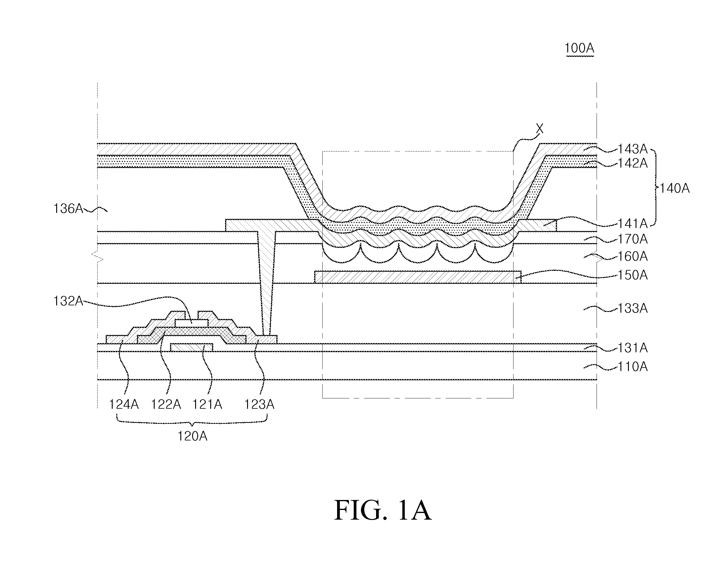
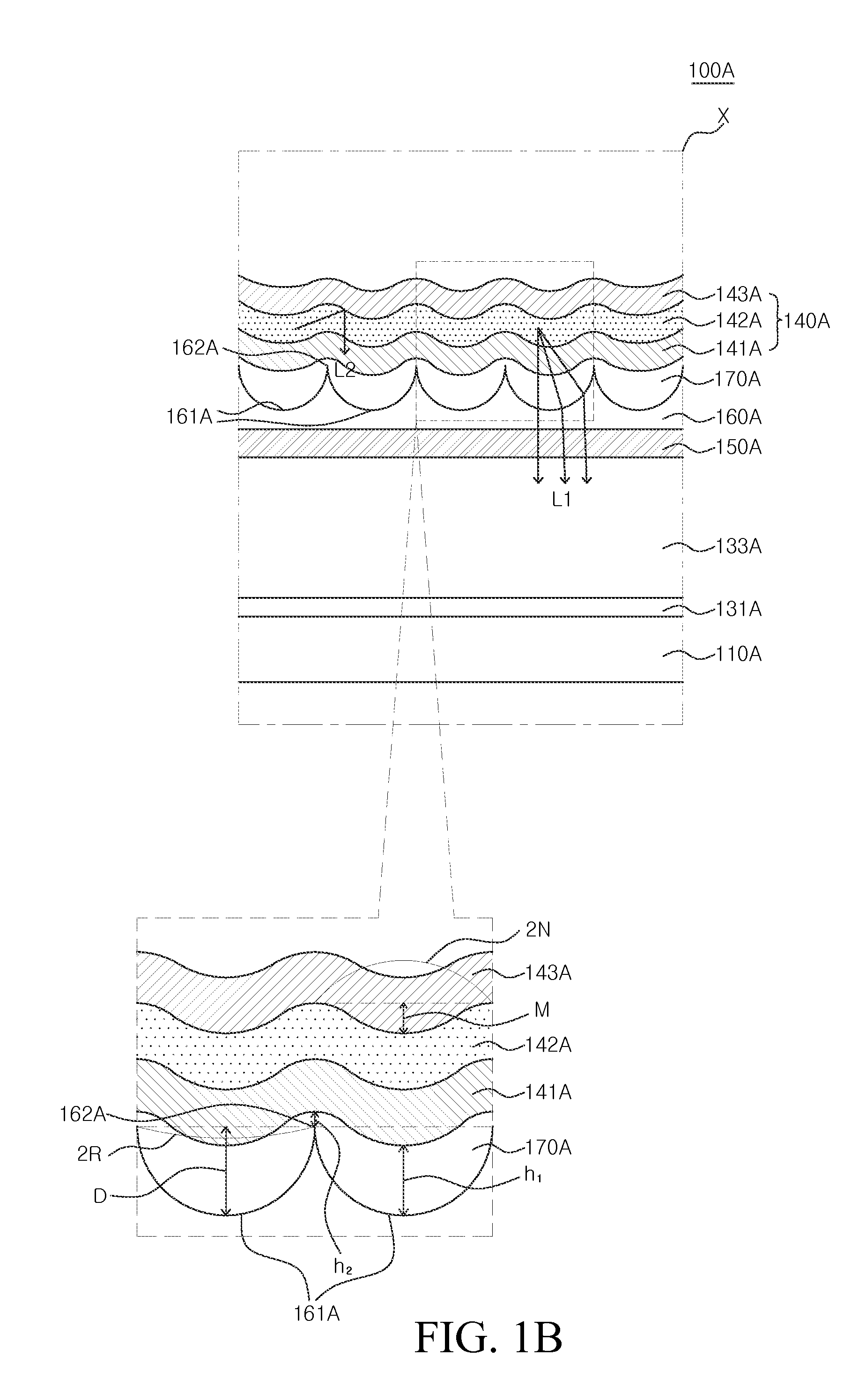
[0012]To achieve these and other advantages and in accordance with the purpose of the present invention, as embodied and broadly described herein, an organic light emitting display device comprises an overcoating layer having a plurality of protrusions or a plurality of recesses; and a buffer layer for reducing step differences. A color filter is disposed on a substrate. The overcoating layer is disposed on the color filter and includes a plurality of protrusions or a plurality of recesses. The plurality of protrusions and the plurality of recesses are disposed on the color filter so as to be overlapped with the color filter. The buffer layer is disposed on the overcoating layer. The buffer layer has a higher refractive index than the overcoating layer and reduces a step difference caused by the plurality of protrusions and the plurality of recesses. An organic light emitting element including an anode, an organic light emitting layer, and a cathode is disposed on the buffer layer. Since the buffer layer for reducing step differences having a higher refractive index than the overcoating layer is disposed between the overcoating layer and the anode, the light emitted from the organic light emitting layer is concentrate in a total reflection critical angle in both of an ITO mode and a substrate mode, enabling multiple reflection of the light. Thus, light extraction efficiency can be increased. Further, since the plurality of protrusions and the plurality of recesses of the overcoating layer are disposed so as to be overlapped with the color filter and disposed between the anode and the color filter, a blurring phenomenon and a ghost phenomenon can be removed and light interference caused by a circular polarizer can also be removed. Further, since the buffer layer for reducing the step difference (or other structural unevenness) is used, it is possible to suppress a short (or other electrical problem) between the anode and the cathode disposed on the overcoating layer.
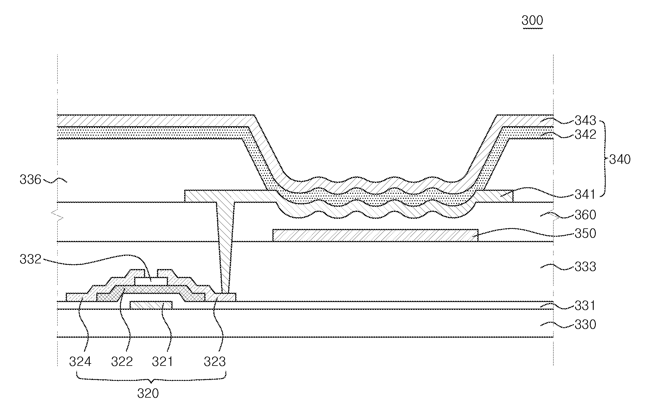
[0013]In another aspect, an organic light emitting display device comprises: a plurality of edge-cut recesses and a filling layer. A color filter is disposed on a substrate. An overcoating layer is disposed on the color filter and includes the plurality of edge-cut recesses. The plurality of edge-cut recesses is disposed on the color filter so as to be overlapped with the color filter and exposes portions of the color filter. The filing layer is disposed on the overcoating layer. The filling layer has a higher refractive index than the overcoating layer and fills at least a part of the inside of the plurality of edge-cut recesses. Each of the plurality of edge-cut recesses has an inclined and curved side surface. An organic light emitting element including an anode, an organic light emitting layer, and a cathode is disposed on the filling layer. Since the filling layer disposed between the overcoating layer and the anode has a higher refractive index than the overcoating layer, it is possible to reduce lights emitted from the organic light emitting layer to be confined in an ITO mode and a substrate mode. Further, since the plurality of edge-cut recesses are disposed so as to expose the color filter, light extraction efficiency in the ITO mode can be improved. Furthermore, since the filling layer fills at least a part of the inside of the plurality of edge-cut recesses, the anode, the organic light emitting layer, and the cathode disposed on the filling layer can be disposed to have an embossed structure. Thus, current efficiency, driving voltage, and power efficiency of the organic light emitting display device can be improved.
[0014]In another aspect, a method for manufacturing an organic light emitting display device including an overcoating layer having a plurality of recesses and a buffer layer for reducing step differences. The method for manufacturing an organic light emitting display device comprises: forming a color filter on a substrate; forming an overcoating layer including a plurality of protrusions or a plurality of recesses disposed on the color filter to be overlapped with the color filter; forming a buffer layer for reducing step differences (or other structural unevenness), which has a higher refractive index than the overcoating layer and reduces a step difference caused by the plurality of protrusions or the plurality of recesses, on the overcoating layer; and forming an organic light emitting element by laminating an anode, an organic light emitting layer, and a cathode in sequence on the buffer layer. Since the buffer layer is formed on the overcoating layer, it is possible to prevent a short between the anode and the cathode formed on the overcoating layer.

Problems solved by technology

However, some of the light emitted from the organic light emitting layer cannot properly output from the organic light emitting display device and may be confined within the organic light emitting display device.
Thus, the organic light emitting display device may have a problem with light extraction efficiency.

Method used


Image

  • Organic light emitting display device and method for manufacturing the same
  • Organic light emitting display device and method for manufacturing the same
  • Organic light emitting display device and method for manufacturing the same

Examples


Embodiment Construction

[0029]Advantages and features of the present disclosure, and methods for accomplishing the same will be more clearly understood from exemplary embodiments described below with reference to the accompanying drawings. However, the present disclosure is not limited to the following exemplary embodiments but may be implemented in various different forms. The exemplary embodiments are provided only to complete disclosure of the present disclosure and to fully provide a person having ordinary skill in the art to which the present disclosure pertains with the category of the invention, and the present disclosure will be defined by the appended claims.

[0030]When an element or layer is referred to as being “on” another element or layer, it may be directly on the other element or layer, or intervening elements or layers may be present.

[0031]Although the terms “first”, “second”, and the like are used for describing various components, these components are not confined by these terms. These ter...


PUM


Abstract

Provided are an organic light emitting display device and a method for manufacturing the same. A color filter is disposed on a substrate. An overcoating layer is disposed on the color filter and includes a plurality of protrusions or a plurality of recesses. The plurality of protrusions and the plurality of recesses are disposed on the color filter to be overlapped with the color filter. A buffer layer for reducing step difference is disposed on the overcoating layer. The buffer layer has a higher refractive index than the overcoating layer and reduces a step difference caused by the plurality of protrusions and the plurality of recesses. An organic light emitting element including an anode, an organic light emitting layer, and a cathode is disposed on the buffer layer. Since the buffer layer has a higher refractive index than the overcoating layer, light extraction efficiency can be increased.

Description

CROSS-REFERENCE TO RELATED APPLICATIONS[0001]This application claims the priority of Korean Patent Application No. 10-2014-0079457 filed on Jun. 27, 2014 and Korean Patent Application No. 10-2014-0150652 filed on Oct. 31, 2014 in the Korean Intellectual Property Office, both of which are hereby incorporated by reference.BACKGROUND OF THE INVENTION[0002]1. Field of the Invention[0003]The present disclosure relates to an organic light emitting display device and a method for manufacturing the same, and more particularly, to an organic light emitting display device improved in light extraction efficiency and a method for manufacturing the same.[0004]2. Description of the Related Art[0005]An organic light emitting display device is a self-light emitting display that does not need a separate light source, like a liquid crystal display device which needs a backlight. Thus, the organic light emitting display device can be manufactured into a light-weight and thin form. Further, the organic...

Claims


Application Information

Patent Timeline
Patent Type & Authority Applications(United States)
IPC IPC(8): H01L27/32H01L51/00H01L51/52H01L51/56
CPCH01L27/3258H01L27/322H01L51/5209H01L51/5275H01L51/5225H01L51/5281H10K59/38H10K59/124H10K50/813H10K50/822H10K50/858H10K50/86H10K59/80515H10K59/80521
Inventor KOO, WONHOEKIM, BONGCHULLEE, KANGJUKIM, SOOKANGJANG, JIHYANGLIM, HYUNSOO
Owner LG DISPLAY CO LTD
Why Eureka
Try Eureka