Methods for forming fin structures with desired dimensions for 3D structure semiconductor applications
a semiconductor and 3d structure technology, applied in the direction of semiconductor devices, electrical equipment, electric discharge tubes, etc., can solve the problems of profile deformation and structure collapse, microloading effect, and additional processing capabilities, and achieve the effect of promoting etching selectivity
- Summary
- Abstract
- Description
- Claims
- Application Information
AI Technical Summary
Benefits of technology
Problems solved by technology
Method used
Image

Examples
Embodiment Construction
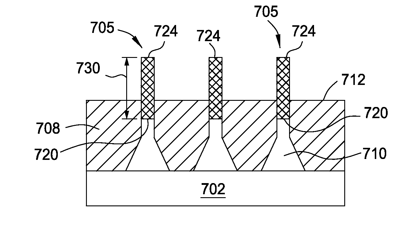
[0028]Methods for forming structures with desired materials, profile and dimensions for three dimensional (3D) stacking of fin field effect transistor (FinFET) for semiconductor chips are provided. The methods utilize an ion implantation process to implant ions into a fin structure forming an etching stop layer to promote etching selectivity. The structure may include a fin structure, a gate structure, a contact structure, or any suitable structure in semiconductor devices, particularly for three dimensional (3D) stacking of fin field effect transistor (FinFET) semiconductor structures. In one embodiment, the ion implantation process is performed to implant dopants into the structure, forming an etching stop interface in the structures. Subsequently, an etching process may be performed to selectively etch the areas with dopants doped therein, without attacking the areas without dopants. An additional material may be later formed on the etched interface to form the structure with com...
PUM
 Abstract
Description
Claims
Application Information
 - Generate Ideas
- Intellectual Property
- Life Sciences
- Materials
- Tech Scout
- Unparalleled Data Quality
- Higher Quality Content
- 60% Fewer Hallucinations
Browse by: Latest US Patents, China's latest patents, Technical Efficacy Thesaurus, Application Domain, Technology Topic, Popular Technical Reports.
© 2025 PatSnap. All rights reserved.Legal|Privacy policy|Modern Slavery Act Transparency Statement|Sitemap|About US| Contact US: help@patsnap.com