Localized stress modulation for overlay and epe

a localized stress and overlay technology, applied in the direction of measurement devices, semiconductor/solid-state device testing/measurement, instruments, etc., can solve the problems of overlay errors, overlay errors, overlay errors of device structure,

Active Publication Date: 2016-01-07
APPLIED MATERIALS INC
View PDF8 Cites 10 Cited by
  • Summary
  • Abstract
  • Description
  • Claims
  • Application Information

AI Technical Summary

Problems solved by technology

However, overlay errors (or pattern registration errors or edge placement errors (EPE)) between layers are inevitable, and error budgets are calculated by IC designers for which the manufacturing must meet.
Overlay errors of the device structure may originate from different error sources, such as overlay errors from previous exposure tool / metrology tool, current exposure tool / metrology tool, a matching error between the overlay errors of the previous exposure tool / metrology tool and of the current exposure tool / metrology tool, or substrate film layer deformation caused by film stress and the like.
As discussed above, displacement or misalignment of the patterns creates overlay errors that may be detriment to device performance.
However, when overlay errors or pattern displacement undesirably occurs, the size, dimension or structures of dies 202, 204, 206 formed on the substrate 200 may be irregularly deformed or distorted, thus increasing likelihood of misalignment between the film layers stacked thereon.
As a result, the probability of misalignment in the subsequent lithographic exposure process may be undesirably increased.
However, this approach often creates logistic problems and adversely decreases throughput.
Furthermore, overlay specifications have become more challenging due to non-lithographic contributions (i.e., film stress).
For example, overlay errors through stress induced substrate distortion may alone exceed the error budget.

Method used


Image

  • Localized stress modulation for overlay and epe
  • Localized stress modulation for overlay and epe
  • Localized stress modulation for overlay and epe

Examples


Embodiment Construction

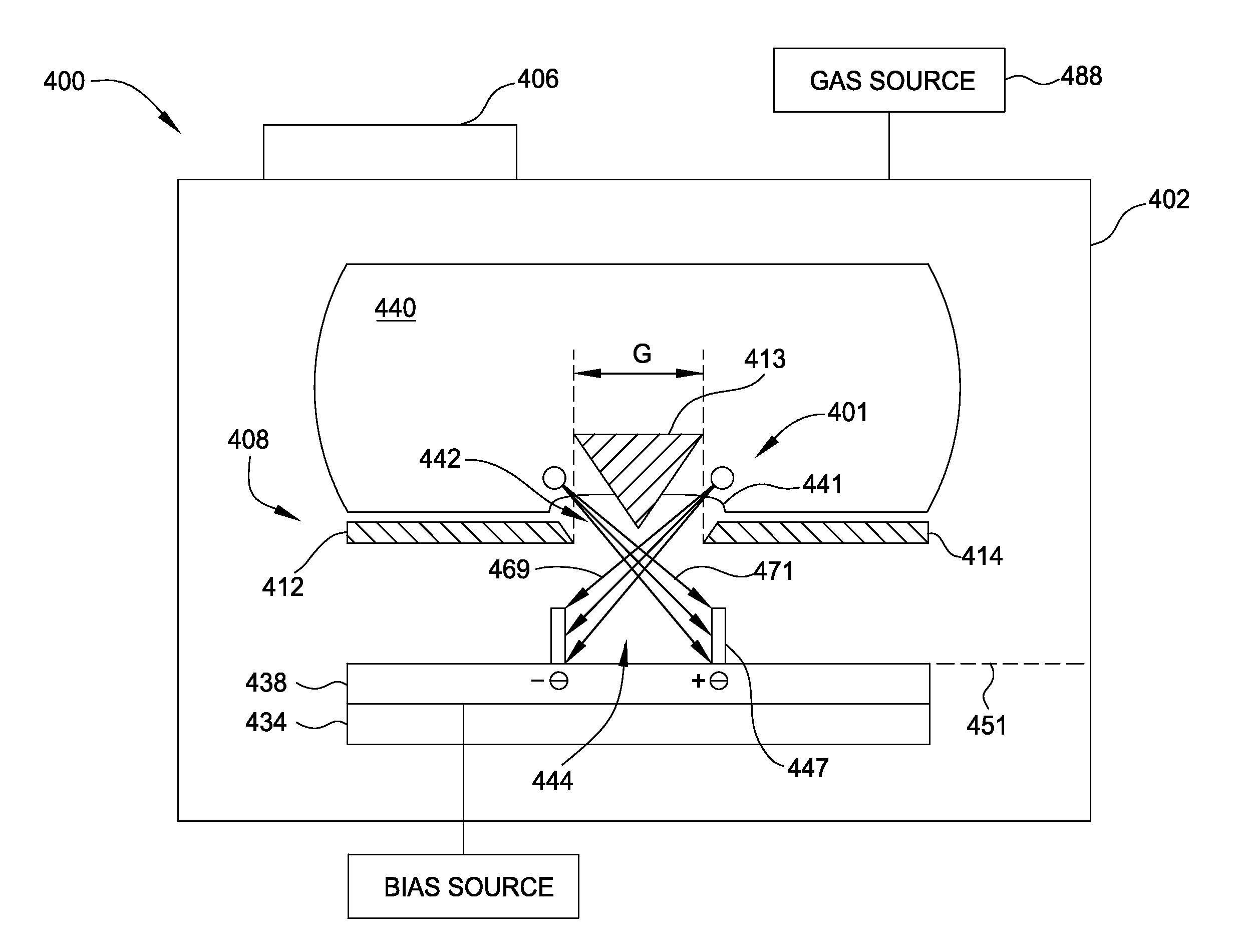
[0023]Embodiments of the disclosure provided herein include apparatus and methods for localized stress modulation, for example, to correct overlay errors and / or edge placement error (EPE). The localized stress modulation process may generally include implantation of ions or electrons while the substrate is disposed within a particle beam generation apparatus.

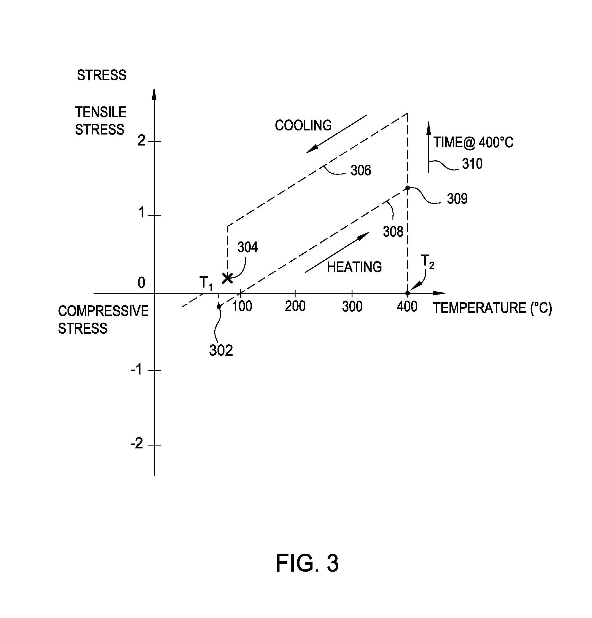
[0024]FIG. 3 depicts a diagram of stress hysteresis of a film layer in response to exposure to thermal process, in accordance with certain aspects of the present disclosure. In the embodiment depicted in FIG. 3, the film layer exposed to the thermal process is a device hardmask layer, such as an amorphous carbon film. It is noted that other types of the film layers, including organic materials, inorganic materials, metal materials, metal dielectric materials, or any other materials that may be utilized to form semiconductor devices may also be tested to record their stress hysteresis to establish database library. Alternatively,...


PUM


Abstract

Embodiments of the disclosure provide apparatus and methods for localized stress modulation for overlay and edge placement error (EPE) using electron or ion implantation. In one embodiment, a process for correcting overlay error on a substrate generally includes performing a measurement process in a metrology tool on a substrate to obtain a substrate distortion or an overlay error map, determining doping parameters to correct overlay error or substrate distortion based on the overlay error map, and providing a doping recipe to a doping apparatus based on the doping parameters determined to correct substrate distortion or overlay error. Embodiments may also provide performing a doping treatment process on the substrate using the determined doping repair recipe, for example, by comparing the overlay error map or substrate distortion with a database library stored in a computing system.

Description

CROSS-REFERENCE TO RELATED APPLICATIONS[0001]This application claims benefit of U.S. Provisional Patent Application No. 62 / 020,244, filed Jul. 2, 2014, the entirety of which is herein incorporated by reference.BACKGROUND[0002]1. Field[0003]Embodiments of the disclosure provided herein generally relate to apparatus and methods for localized stress modulation, for example, to correct overlay error and edge placement error (EPE).[0004]2. Description of the Related Art[0005]In the manufacture of integrated circuits (IC), or chips, patterns representing different layers of the chip are created by a chip designer. A series of reusable masks, or photomasks, are created from these patterns in order to transfer the design of each chip layer onto a semiconductor substrate during the manufacturing process. Mask pattern generation systems use precision lasers or electron beams to image the design of each layer of the chip onto a respective mask. The masks are then used much like photographic ne...

Claims


Application Information

Patent Timeline
Patent Type & Authority Applications(United States)
IPC IPC(8): H01L21/66
CPCH01L22/12H01L22/20
Inventor YIEH, ELLIE Y.DAI, HUIXIONGNEMANI, SRINIVAS D.GODET, LUDOVICBENCHER, CHRISTOPHER DENNIS
Owner APPLIED MATERIALS INC
Why Eureka
Try Eureka