

Autobahn interconnect in IC with multiple conduction lanes
a technology of interconnection and conduction lanes, applied in the direction of semiconductor devices, semiconductor/solid-state device details, non-conductive materials with dispersed conductive materials, etc., can solve the problem of limiting the performance of the device, achieve the effect of avoiding random scattering, limiting the device performance, and lowering the dispersion
- Summary
- Abstract
- Description
- Claims
- Application Information
AI Technical Summary
Benefits of technology
Problems solved by technology
Method used
Image

Examples
Embodiment Construction
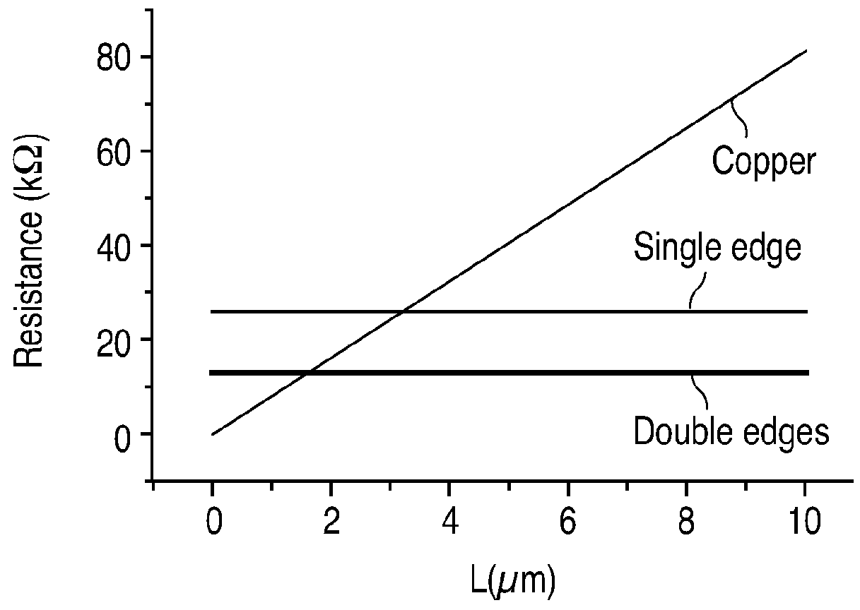
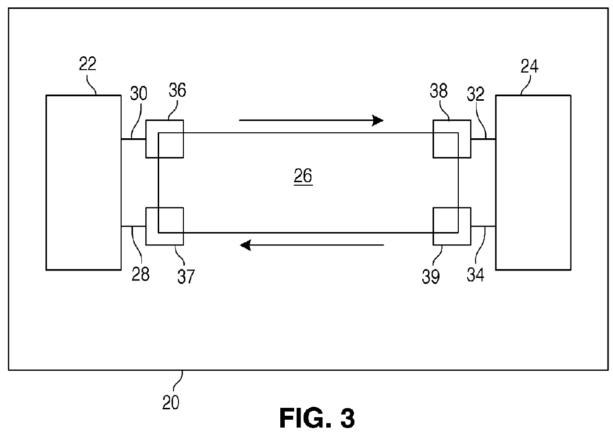
[0009]In accordance with the principles of the present invention, an electrical device incorporates a magnetic TI layer as an interconnect layer in an integrated circuit and includes at least one electrode in electrical contact with the edge of the magnetic TI layer.
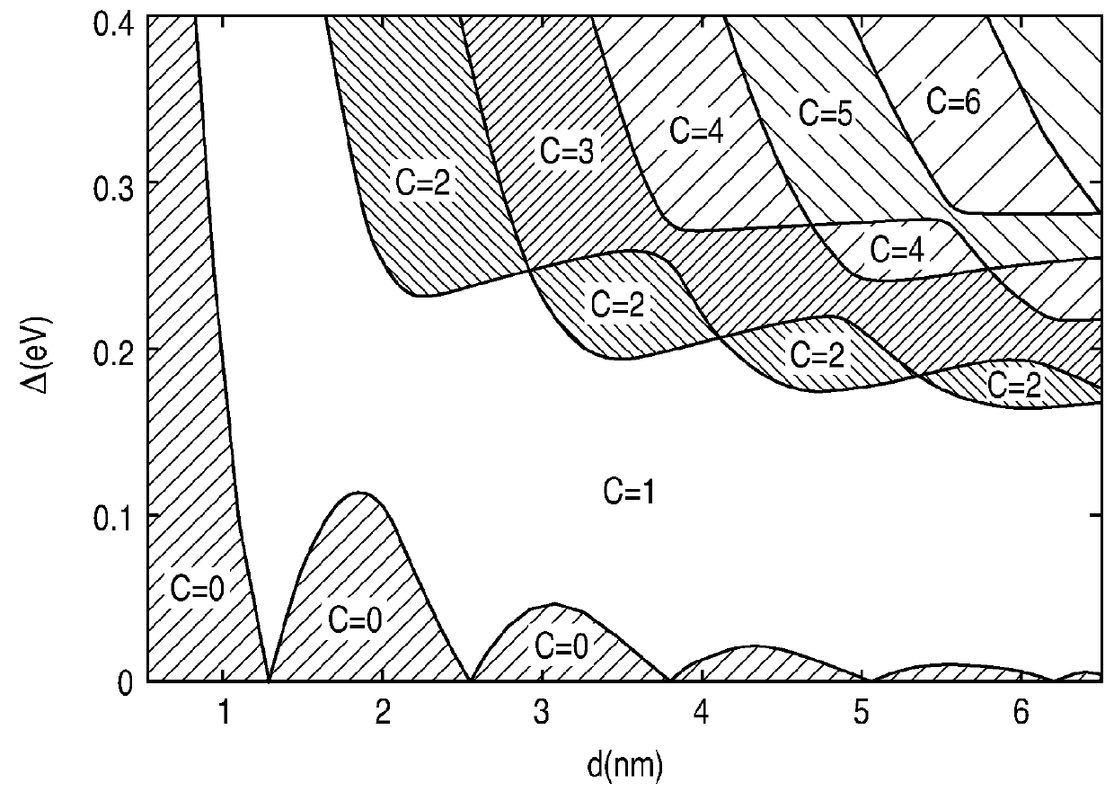
[0010]In the present description, a topological insulator, in two or three dimensions, is a material having insulating energy gaps in the bulk and gapless edge or surface states on the sample boundary that are protected by time-reversal symmetry. That is, a topological insulator is a material with a bulk insulating gap and a conducting surface state protected from any time reversal invariant perturbation. In the present description, gapless edge or surface states refer to an edge or surface states having a zero bandgap. In other words, a topological insulator is a material that behaves as an insulator in its interior while permitting the movement of charges on its boundary. Furthermore, the surface states of a topologica...
PUM
 Abstract
Description
Claims
Application Information