Insulated gate semiconductor device

a technology semiconductor element, which is applied in the direction of electronic switching, power conversion systems, pulse techniques, etc., can solve the problems of high short circuit capacity detection of short circuits of loads, and inability to cause insulated gate semiconductor elements to operate, etc., to prevent the heat generation prevent the overheating destruction of insulated gate semiconductor elements, and prevent the effect of detection simpl

Active Publication Date: 2016-02-04
FUJI ELECTRIC CO LTD
View PDF5 Cites 6 Cited by
  • Summary
  • Abstract
  • Description
  • Claims
  • Application Information

AI Technical Summary

Benefits of technology

[0019]In the insulated gate semiconductor device of the described configuration, by focusing attention on the on-voltage of the insulated gate semiconductor element, it is determined whether an increase in the output current is a temporary one responding to the condition of the load or results from a short circuit of the load. Further, when the on-voltage is lower than the first threshold voltage and the increase in the output current is a temporary one, the gate voltage to be applied to the control terminal of the insulated gate semiconductor element is raised, while the on-resistance of the insulated gate semiconductor element is lowered. As a result, it is possible to prevent a heat generation of the insulated gate semiconductor element resulting from the increase in the output current, and prevent an overheat destruction of the insulated gate semiconductor element.
[0020]Consequently, there is no need to construct an insulated gate semiconductor device using, for example, an insulated gate semiconductor element having an excessive current capacity compared with th

Problems solved by technology

However, a device using the insulated gate semiconductor element, unlike the device using the junction FET, cannot cause the insulated gate semiconductor element to operate by switching between the unipolar mode and the bipolar mode.
However, an insulated

Method used


Image

  • Insulated gate semiconductor device
  • Insulated gate semiconductor device
  • Insulated gate semiconductor device

Examples


Embodiment Construction

[0026]Hereafter, a description will be given, referring to the drawings, of an insulated gate semiconductor device according to one embodiment.

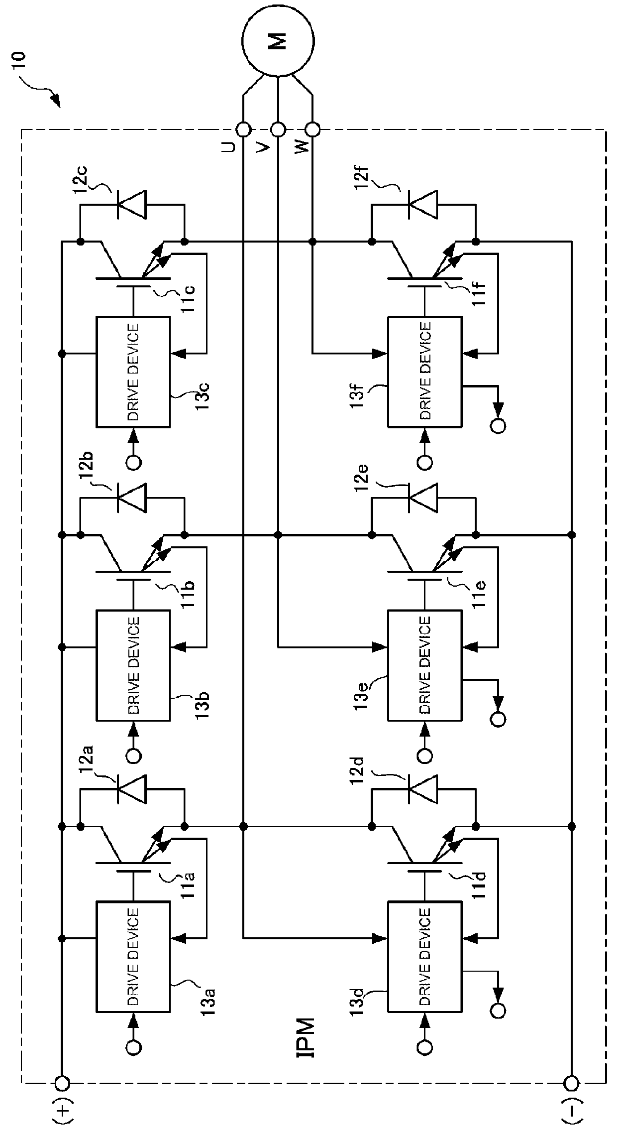
[0027]The insulated gate semiconductor device is realized as, for example, an inverter device 10 which supplies a drive current to a three-phase alternating current motor M, as shown in FIG. 1. The inverter device 10 includes a power semiconductor module packaged including six IGBTs 11a to 11f as insulated gate semiconductor elements large in power capacity. The six IGBTs 11a to 11f configure the main part of the inverter device 10 which drives the three-phase alternating current motor M acting as a load. The inverter device 10 supplies a drive current to the three-phase alternating current motor M by driving the plurality of IGBTs 11a to 11f on and off, with the IGBTs 11a to 11f correlated with each other, using an unshown control circuit.

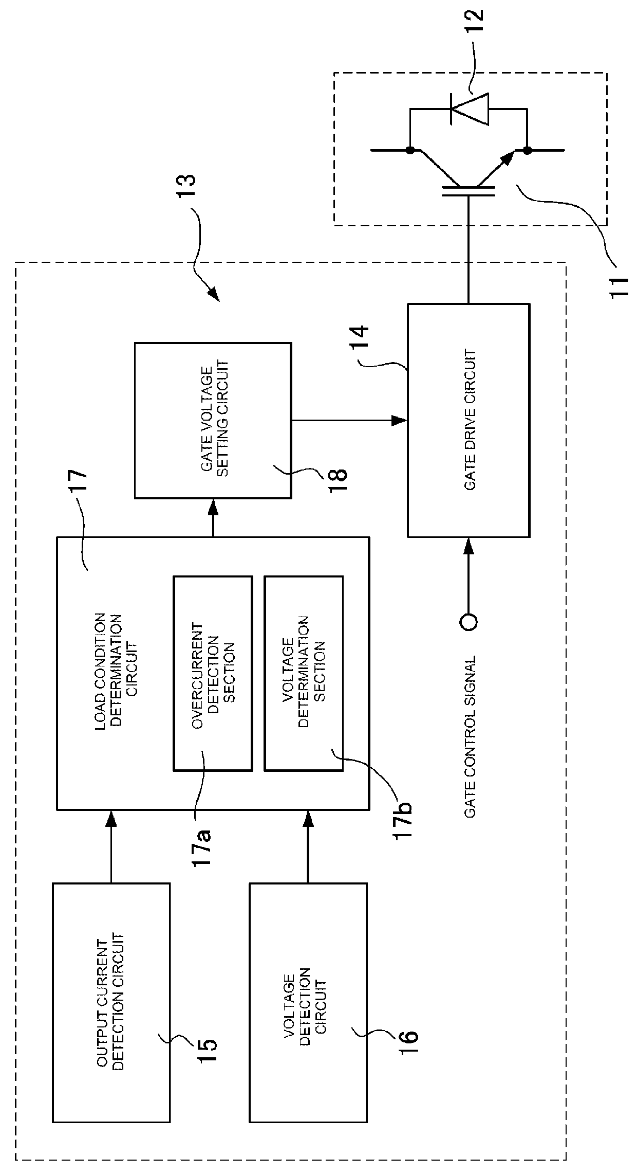
[0028]Incidentally, the six IGBTs 11a and 11b to 11f are connected in pairs in series to form three half...


PUM


Abstract

An insulated gate semiconductor device includes an insulated gate semiconductor element, an output current detection unit, a voltage detection unit, and a heat generation amount suppression unit. The insulated gate semiconductor element on-operates by receiving a first gate voltage at a control terminal, and switches and outputs an input voltage to a load. The output current detection unit detects an output current to the load. The voltage detection unit detects an on-voltage of the insulated gate semiconductor element. The heat generation amount suppression unit sets a gate voltage to be applied to the control terminal of the insulated gate semiconductor element higher than the first gate voltage in response to the output current exceeding a rated current value and the on-voltage being lower than a first threshold voltage.

Description

CROSS-REFERENCE TO RELATED APPLICATION[0001]This application is a Continuation of International Application PCT / JP2014 / 066907 filed on Jun. 25, 2014, and claims priority to, Japanese Patent Application No. 2013-198206, filed on Sep. 25, 2013, the contents of both of which are entirely incorporated herein by reference for all purposes.BACKGROUND[0002]1. Technical Field[0003]The present disclosure relates to an insulated gate semiconductor device which supplies power to a load by switching an insulated gate semiconductor element, such as an IGBT or a power MOS-FET.[0004]2. Description of Related Art[0005]As a drive device which drives a load such as a motor, a semiconductor device which, by switching and driving a semiconductor element such as a transistor, converts input power to power suitable for driving the load, is known. FIG. 4 is a main portion outline configuration diagram showing one example of this kind of semiconductor device 1 which is introduced in detail in, for example,...

Claims


Application Information

Patent Timeline
IPC IPC(8): H02M1/088H02M7/5387H03K17/082
CPCH02M1/088H03K17/0828H02M7/53871H02M1/08H02M7/5387H03K17/06H03K2017/0806H02M1/327H02M7/00H02M7/21
Inventor MOMOTA, SEIJI
Owner FUJI ELECTRIC CO LTD
Why Eureka
Try Eureka