Blind Via Printed Circuit Board Fabrication Supporting Press Fit Connectors

Active Publication Date: 2016-02-18
DELL SOFTWARE +2
View PDF5 Cites 3 Cited by
  • Summary
  • Abstract
  • Description
  • Claims
  • Application Information

AI Technical Summary

Benefits of technology

[0010]In accordance with the present invention, a system and method are provided which substantially reduce the disadvantages and problems associated with previous methods and systems for colocation of press fit connectors and surface mounted connectors at opposing sides of a circuit board. A counter bore opening in the bottom of a blind via that passes plating fluid through during manufacture of a first circuit board portion is covered by a blocking material to prevent fluids from entering the blind via through the opening during lamination of a second circuit board portion to the first circuit board portion over the opening.
[0011]More specifically, an information handling system motherboard with a storage device controller interfaces to a storage device circuit board through a press in connector coupled to the storage device circuit board. The press in connector communicates signals from the storage device controller through the circuit board to a surface connector that couples with a storage device. In order to provide freedom of placement of the surface connector and press in connector on opposing sides of the storage device circuit board, such as colocation on opposite sides, the storage device circuit board is assembled from first and second circuit board portions. The first portion has blind vias formed with a small diameter opening in the bottom of each blind via that allows plating fluid to pass through. After plating of the blind vias with conductive material, the openings in the bottom of the blind vias are blocked with a blocking material, such as by printing ink across the openings. The

Problems solved by technology

One difficulty with upper and lower surface connector configurations is that press fit connectors are inserted into relatively large through hole vias in the mid-plane circuit board.
However, including a second set of press fit connectors to interface the two mi

Method used


Image

  • Blind Via Printed Circuit Board Fabrication Supporting Press Fit Connectors
  • Blind Via Printed Circuit Board Fabrication Supporting Press Fit Connectors
  • Blind Via Printed Circuit Board Fabrication Supporting Press Fit Connectors

Examples


Embodiment Construction

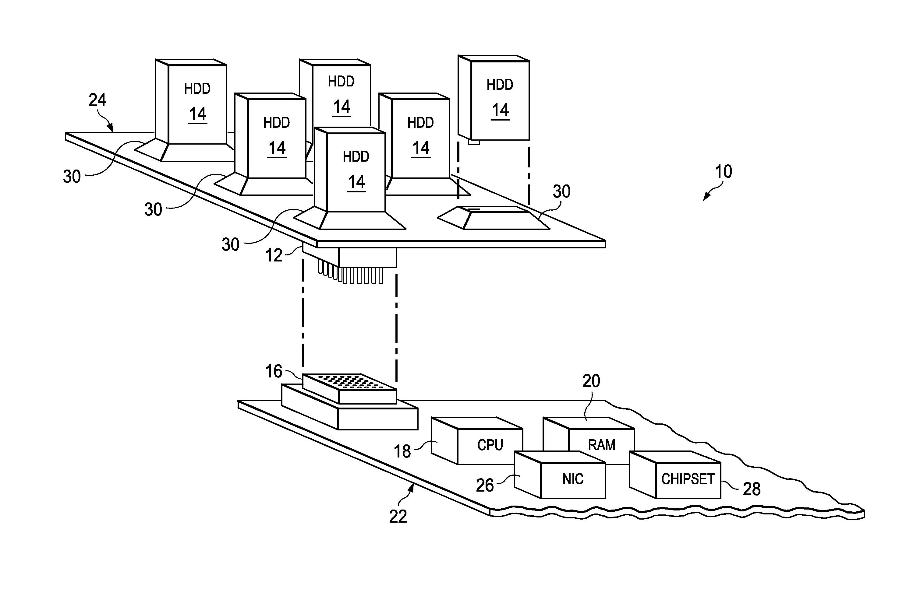
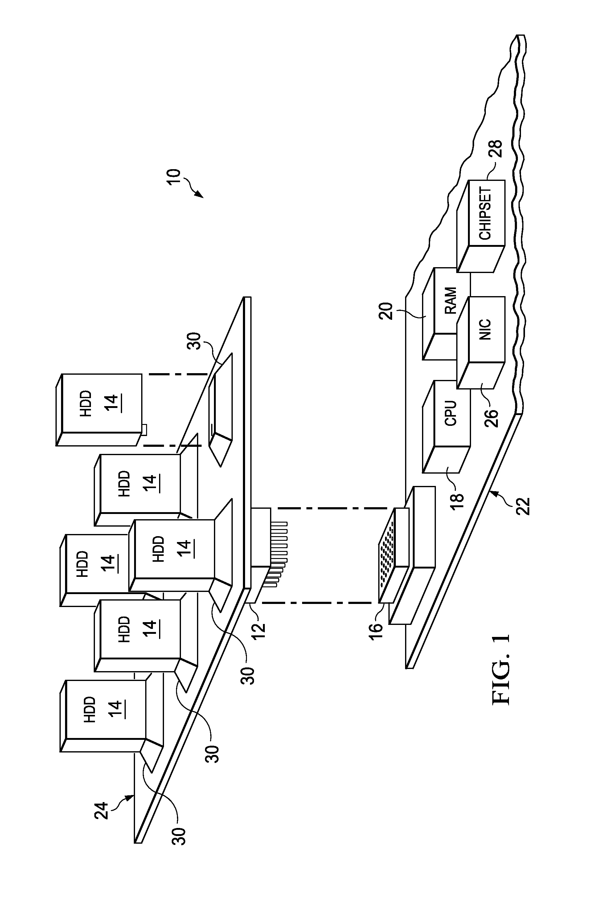
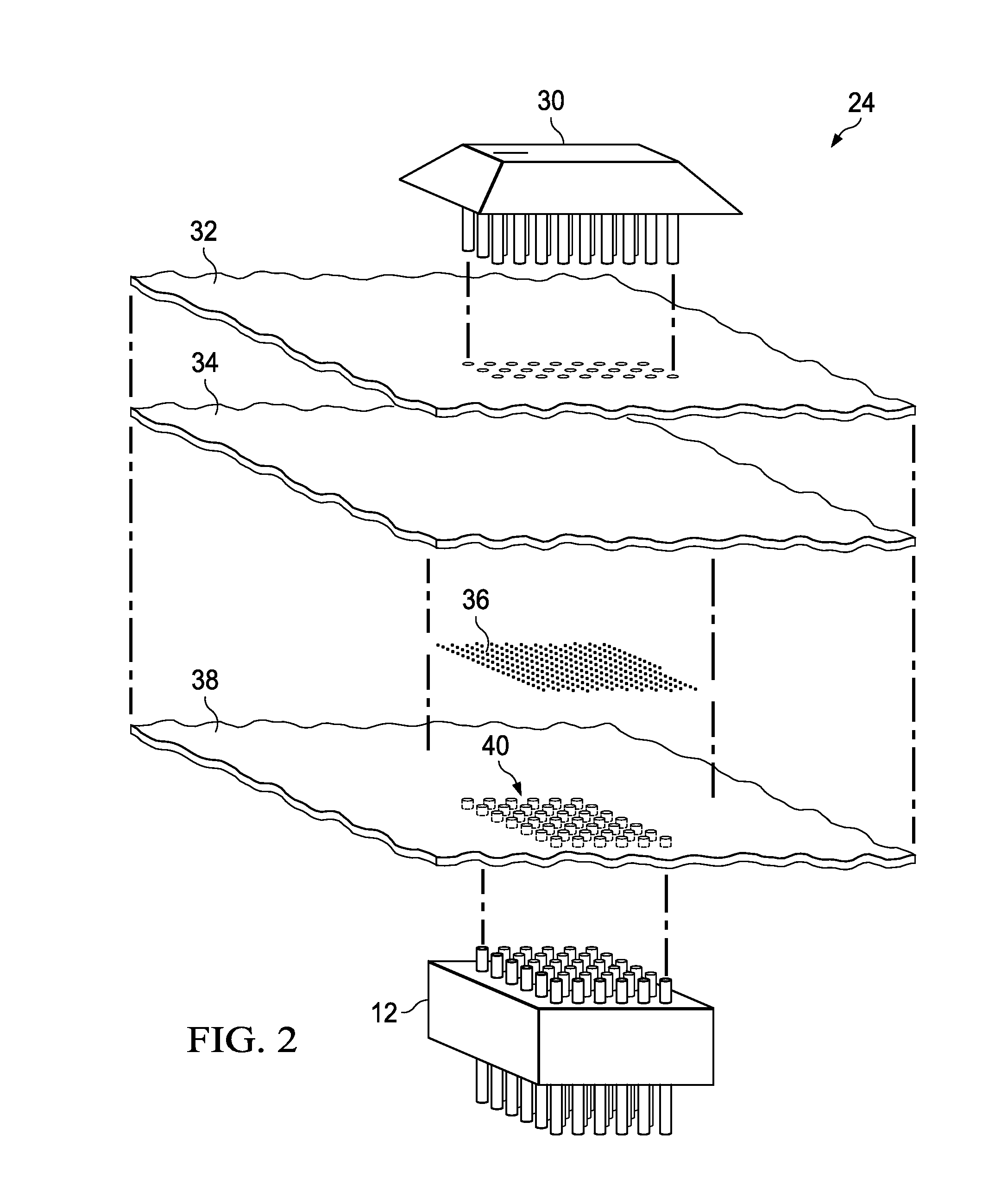
[0022]Blind vias of an information handling system circuit board accept a press in connector and a surface connector collocated on opposing surfaces. For purposes of this disclosure, an information handling system may include any instrumentality or aggregate of instrumentalities operable to compute, classify, process, transmit, receive, retrieve, originate, switch, store, display, manifest, detect, record, reproduce, handle, or utilize any form of information, intelligence, or data for business, scientific, control, or other purposes. For example, an information handling system may be a personal computer, a network storage device, or any other suitable device and may vary in size, shape, performance, functionality, and price. The information handling system may include random access memory (RAM), one or more processing resources such as a central processing unit (CPU) or hardware or software control logic, ROM, and / or other types of nonvolatile memory. Additional components of the i...


PUM

PropertyMeasurementUnit
Electrical conductoraaaaaaaaaa
Widthaaaaaaaaaa

Abstract

An information handling system circuit board interfaces storage device surface connectors and storage device controllers disposed on opposing sides by coupling a first circuit board portion having a controller press in connector to a second circuit board portion having plural surface connectors. The first and second circuit board portions couple to each other with an adhesive activated by curing. Resistant ink is printed over openings of the first circuit board portion where adhesive is applied in order to prevent the adhesive from flowing into the openings at or before the curing of the adhesive.

Description

CROSS-REFERENCE TO RELATED APPLICATIONS[0001]This application is a continuation of co-pending application Ser. No. 13 / 628,532, filed Sep. 27, 2012, which is incorporated herein by reference in its entirety.BACKGROUND OF THE INVENTION[0002]1. Field of the Invention[0003]The present invention relates in general to the field of information handling system circuit boards, and more particularly to blind via printed circuit board fabrication supporting press fit connectors.[0004]2. Description of the Related Art[0005]As the value and use of information continues to increase, individuals and businesses seek additional ways to process and store information. One option available to users is information handling systems. An information handling system generally processes, compiles, stores, and / or communicates information or data for business, personal, or other purposes thereby allowing users to take advantage of the value of the information. Because technology and information handling needs ...

Claims


Application Information

Patent Timeline
IPC IPC(8): H05K1/11H01R12/70H05K3/00H05K3/36H05K3/42
CPCH05K1/115H01R12/7076H05K3/0047H05K2201/09545H05K3/36H05K3/421H05K2201/09509H05K3/0094H01R12/585H05K3/306H05K3/4611H05K2201/09845H05K2201/10189H05K2201/10545H05K2203/1476Y10T29/49126
Inventor MUNDT, KEVIN W.ADRIAN, JASON D.
Owner DELL SOFTWARE
Why Eureka
Try Eureka