
Film-forming and analysis composite apparatus, method for controlling film-forming and analysis composite apparatus, and vacuum chamber

Inactive Publication Date: 2016-02-25
SHARP KK
View PDF2 Cites 0 Cited by
  • Summary
  • Abstract
  • Description
  • Claims
  • Application Information

AI Technical Summary

Benefits of technology

The patent is about a machine that can quickly and accurately get information about a sample. It has two parts: a part that forms a film on the sample using sputtering, and a part that analyzes the film using spectroscopic analysis. These parts are connected by a vacuum chamber that creates a vacuum inside. The machine can create a vacuum inside the chamber and use the interrupting member to separate the two spaces. This allows for communication between the two spaces. The technical effect of this patent is to provide a more efficient and flexible machine for analyzing samples.

Problems solved by technology

However, there are problems in that mobility is small in a-Si:H and local non-uniformity which occurs during crystallization is generated in LTPS.
However, with the method according to Japanese Unexamined Patent Application Publication No. 2012-33857, in a case of determining that an abnormality is generated in the mobility of an oxide semiconductor thin film, it is not possible to determine whether the abnormality is generated (i) due to deviation in the composition ratio of the oxide semiconductor thin film or (ii) due to an abnormality in the bonding state.
That is, there is a problem in that it is not possible to obtain accurate information about the oxide semiconductor thin film to the extent of being able to specify the cause of an abnormality.
Furthermore, since a sample, on which an oxide semiconductor thin film is film-formed, has to be exposed to the atmosphere at least once during evaluation, there is also a problem in that it is not possible to obtain accurate information about the oxide semiconductor thin film in a case where the surface of the oxide semiconductor thin film is contaminated.
Furthermore, there is a problem in that it is not possible to quickly obtain information about the oxide semiconductor thin film.
In addition, with the method according to Japanese Unexamined Patent Application Publication No. 2003-201562, it is not possible to directly monitor the film composition of the film-formed oxide semiconductor thin film and it is not possible to discover whether the composition is minutely changed in the film-formed oxide semiconductor thin film.
That is, there is a problem in that it is not possible to obtain accurate information about the oxide semiconductor thin film.
Thus, with the methods according to Japanese Unexamined Patent Application Publication No. 2012-33857 and Japanese Unexamined Patent Application Publication No. 2003-201562, there is a problem in that it is not possible to quickly and accurately obtain information about a sample (in particular, oxide semiconductor thin films).

Method used


Image

  • Film-forming and analysis composite apparatus, method for controlling film-forming and analysis composite apparatus, and vacuum chamber
  • Film-forming and analysis composite apparatus, method for controlling film-forming and analysis composite apparatus, and vacuum chamber
  • Film-forming and analysis composite apparatus, method for controlling film-forming and analysis composite apparatus, and vacuum chamber

Examples


embodiment 1

[0037]Description will be given of Embodiment 1 of the disclosure based on FIG. 1 to FIG. 7.

Configuration of Vacuum Chamber 1

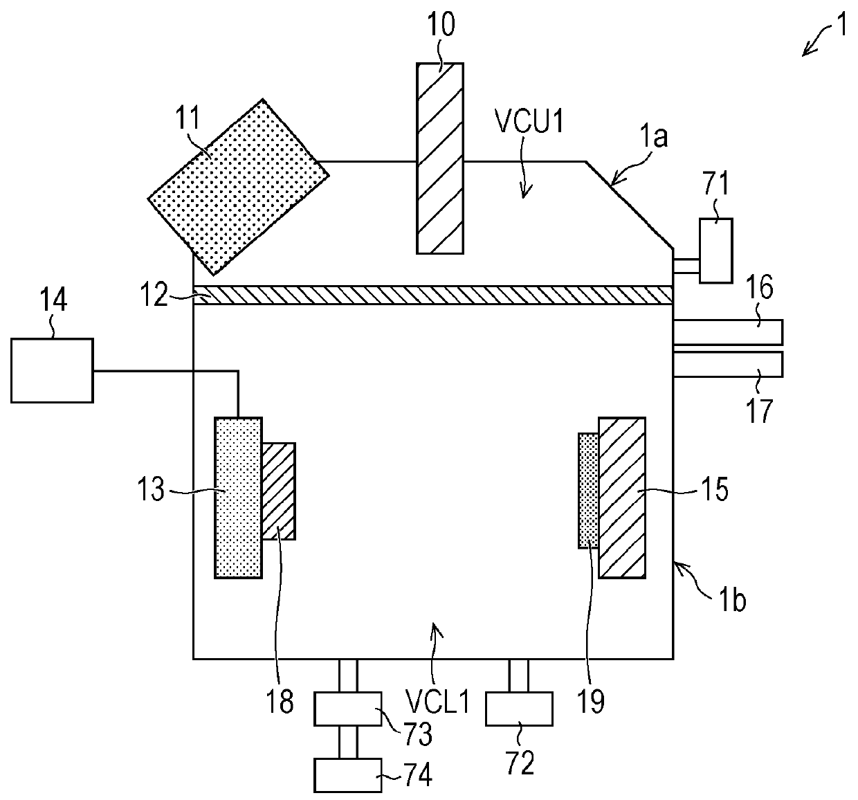
[0038]FIG. 1 is a diagram which shows a configuration of a vacuum chamber 1 (a film-forming and analysis composite apparatus) of the present embodiment. As described below, the vacuum chamber 1 is configured as a film-forming and analysis composite apparatus in which an analysis apparatus 1a and a film-forming apparatus 1b are combined.

[0039]Accordingly, it may be understood that the vacuum chamber 1 of the present embodiment is a film-forming and analysis composite apparatus having a function as a vacuum chamber which can make an inner space thereof a vacuum.

[0040]The vacuum chamber 1 is configured so as to be able to film-form an oxide semiconductor thin film (a sample) and perform spectroscopic analysis using X-ray photoelectron spectroscopy (XPS) with respect to the oxide semiconductor thin film. The vacuum chamber 1 is provided with the analysis apparatus...

embodiment 2

[0107]Description will be given of another embodiment of the disclosure based on FIG. 8 and FIGS. 9A to 9C. Here, for convenience of description, the same reference numerals are given to members which have the same functions as the members described in the previous embodiment and description thereof will be omitted.

Configuration of Vacuum Chamber 2

[0108]FIG. 8 is a diagram which shows a configuration of a vacuum chamber 2 (a film-forming and analysis composite apparatus) of the present embodiment. The vacuum chamber 2 of the present embodiment has a configuration which is realized by replacing the analysis apparatus 1a of Embodiment 1 with an analysis apparatus 2a. Then, the analysis apparatus 2a of the present embodiment has a configuration which is realized by adding an argon ion gun 29 (an ion gun) to the analysis apparatus 1a of Embodiment 1.

[0109]The argon ion gun 29 irradiates an oxide semiconductor thin film with argon ions (etching ions). The oxide semiconductor thin film is...

embodiment 3

[0125]Description will be given of another embodiment of the disclosure based on FIG. 10 to FIG. 15. Here, for convenience of description, the same reference numerals are given to members which have the same functions as the members described in the previous embodiments and description thereof will be omitted.

Configuration of Vacuum Chamber 3

[0126]FIG. 10 is a diagram which shows a configuration of a vacuum chamber 3 (a film-forming and analysis composite apparatus) of the present embodiment. The vacuum chamber 3 of the present embodiment has a configuration which is realized by replacing the analysis apparatus 1a of Embodiment 1 with an analysis apparatus 3a.

[0127]Then, the analysis apparatus 3a of the present embodiment has a configuration which is realized by (i) replacing the X-ray source 10 with an electron gun 30 (an inspection radiation source) and replacing the photoelectron detector 11 with an Auger electron detector 31 (an electron detector) and (ii) adding a secondary el...


PUM


Abstract

A vacuum chamber is provided with a film-forming apparatus which film-forms an oxide semiconductor thin film by sputtering, an analysis apparatus which performs spectroscopic analysis with respect to a surface of the film-formed oxide semiconductor thin film, and a valve which splits an inner space of the vacuum chamber into a first space where the analysis apparatus is arranged and a second space where the film-forming apparatus is arranged and permits communication between the split first space and second space.

Description

BACKGROUND[0001]1. Field[0002]The present disclosure relates to a film-forming and analysis composite apparatus in which a film-forming apparatus and an analysis apparatus are combined.[0003]2. Description of the Related Art[0004]In recent years, active matrix type liquid crystal display apparatuses where a thin film transistor (TFT) is arranged in each pixel of a liquid crystal display apparatus have been widely used.[0005]In addition, hydrogenated amorphous silicon (a-Si:H), low temperature poly silicon (LTPS), and the like have been mainly used as the semiconductor material of the TFT.[0006]However, there are problems in that mobility is small in a-Si:H and local non-uniformity which occurs during crystallization is generated in LTPS. For this reason, oxide semiconductors which are represented by oxides which include indium (In), gallium (Ga), and zinc (Zn) have recently attracted attention. Using these oxide semiconductors, it is possible to obtain high mobility even at room tem...

Claims


Application Information

Patent Timeline
IPC IPC(8): G01N23/227
CPCG01N2223/6116G01N23/2273
Inventor NIINOH, ATSUSHI
Owner SHARP KK
Learn More