Verification Of Photonic Integrated Circuits

a photonic integrated circuit and verification technology, applied in the field of layout design data analysis, can solve the problems of not fully addressing the adapting an eda flow developed for electronic ic designs to the specific needs of pic designs, and the difficulty of applying various aspects of this flow to the photonic integrated circui

Active Publication Date: 2016-02-25
SIEMENS PROD LIFECYCLE MANAGEMENT SOFTWARE INC
View PDF9 Cites 15 Cited by
  • Summary
  • Abstract
  • Description
  • Claims
  • Application Information

AI Technical Summary

Benefits of technology

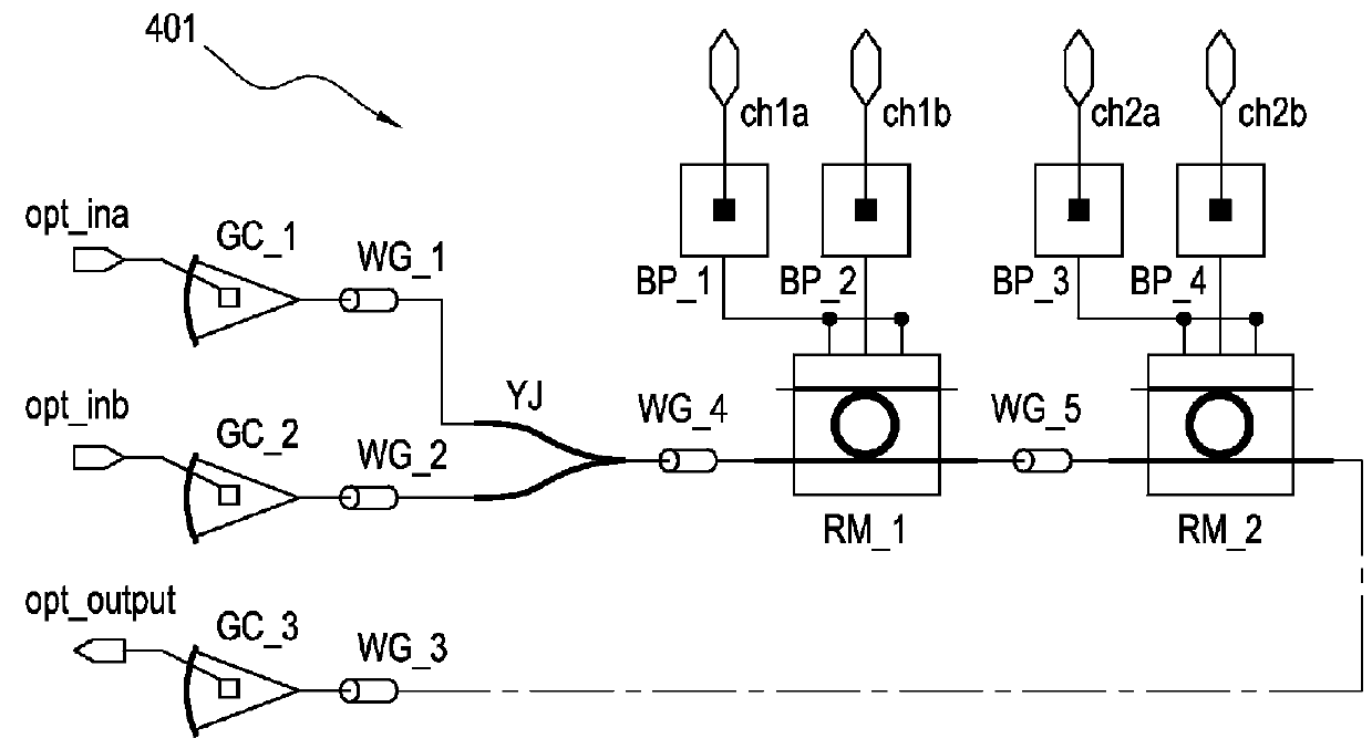
[0011]Aspects of the invention relate to mechanisms for the use of layout-versus-schematic (LVS) design tools to validate photonic integrated circuit designs where the conventional integrated circuit design flow cannot be applied directly to or perform checks that are specific to photonic circuits. Various implementations of the invention employ alternate analysis techniques with LVS analysis tools to perform one or more LVS analysis processes on photonic integrated circuits. These analysis processes may include curvilinear design validation and the associated flow implementations.

Problems solved by technology

While the conventional design flow process described above is applicable to a variety of microdevices, it is difficult to apply various aspects of this flow to photonic integrated circuits, and the issues of adapting an EDA flow developed for electronic IC designs to the specific needs of PIC designs have not yet been fully addressed.

Method used


Image

  • Verification Of Photonic Integrated Circuits
  • Verification Of Photonic Integrated Circuits
  • Verification Of Photonic Integrated Circuits

Examples


Embodiment Construction

Illustrative Operating Environment

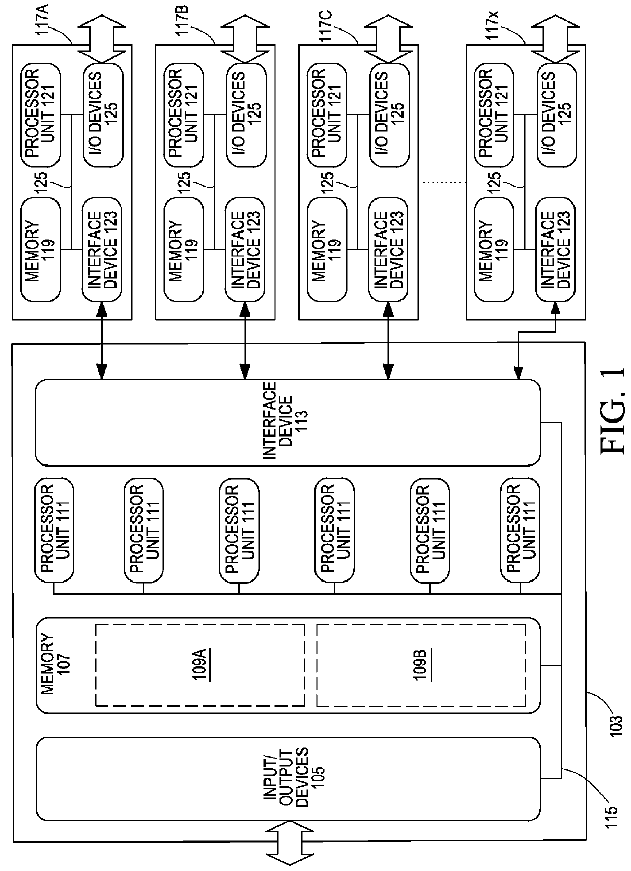
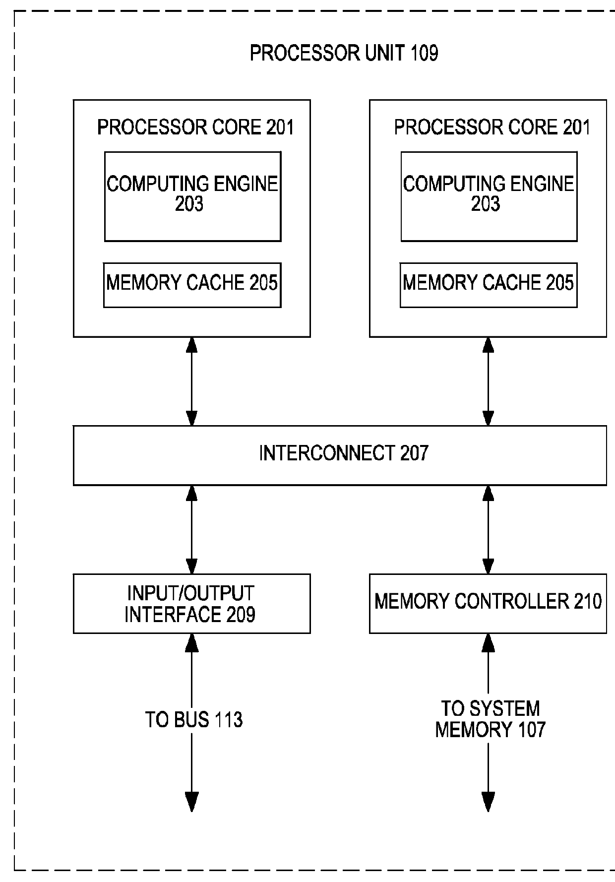
[0019]The execution of various electronic design automation processes according to embodiments of the invention may be implemented using computer-executable software instructions executed by one or more programmable computing devices. Because these embodiments of the invention may be implemented using software instructions, the components and operation of a generic programmable computer system on which various embodiments of the invention may be employed will first be described. Further, because of the complexity of some electronic design automation processes and the large size of many circuit designs, various electronic design automation tools are configured to operate on a computing system capable of simultaneously running multiple processing threads. The components and operation of a computer network having a host or master computer and one or more remote or servant computers therefore will be described with reference to FIG. 1. This operating en...


PUM


Abstract

Techniques and mechanisms for the use of layout-versus-schematic (LVS) design tools to validate photonic integrated circuit designs. Various implementations employ alternate analysis techniques with LVS analysis tools to perform one or more LVS analysis processes on photonic integrated circuits. These analysis processes may include curvilinear design validation and the associated flow implementations.

Description

RELATED APPLICATIONS[0001]This application claims priority under 35 U.S.C. §119 to U.S. Provisional Patent Application No. 61 / 982,329, filed on Apr. 22, 2014, entitled “Photonics Design With An EDA Approach: Validation Of Layout Waveguide Interconnects,” and naming Ruping Cao as inventor, which application is incorporated entirely herein by reference. This application also claims priority under 35 U.S.C. §119 to U.S. Provisional Patent Application No. 62 / 151,240, filed on Apr. 22, 2015, entitled “LVS Check For Photonic Integrated Circuits—Curvilinear Feature Extraction And Validation,” and naming Ruping Cao et al. as inventors, which application is incorporated entirely herein by reference as well.FIELD OF THE INVENTION[0002]The present invention is directed to the analysis of layout design data representing photonic integrated circuit devices. Various implementations of the invention may be particularly useful for validating a photonic integrated circuit design.BACKGROUND OF THE IN...

Claims


Application Information

Patent Timeline
Patent Type & Authority Applications(United States)
IPC IPC(8): G06F17/50
CPCG06F17/5081G06F30/398
Inventor CAO, RUPINGFERGUSON, JOHN G.CAYO, JOHN D.ARRIORDAZ, ALEXANDRE
Owner SIEMENS PROD LIFECYCLE MANAGEMENT SOFTWARE INC
Why Eureka
Try Eureka