Under-fill material, sealing sheet, and method for producing semiconductor device

a technology of sealing sheet and semiconductor device, which is applied in the direction of synthetic resin layered products, other domestic products, chemical processes, etc., can solve the problems of difficult adjustment of injection position and injection amount of liquid sealing resin, and achieve the effect of correct positioning, satisfactory yield ratio, and accurate and easy and convenient operation

Inactive Publication Date: 2016-03-03
NITTO DENKO CORP
View PDF3 Cites 5 Cited by
  • Summary
  • Abstract
  • Description
  • Claims
  • Application Information

AI Technical Summary

Benefits of technology

[0008]Regarding registration during mounting, a sheet-shaped under-fill material is laminated on a semiconductor element beforehand, and therefore the under-fill material is required to have transparency which ensures that an alignment mark provided on the semiconductor element can be recognized at the time of alignment of the semiconductor element and the substrate during mounting of the semiconductor element. However, when a silica filler or the like is added to the under-fill material for reducing a difference in thermal expansion coefficient between the semiconductor element and the adherend, the transparency of the under-fill material is reduced, so that it maybe difficult to perform alignment of the semiconductor element and the substrate during mounting of the semiconductor element.
[0022]In the production method, a predetermined under-fill material is used, and therefore an alignment mark provided on the semiconductor element or the adherend can be precisely recognized. Accordingly, position matching can be correctly and easily and conveniently performed at the time of mounting the semiconductor element on the adherend, and a semiconductor device can be produced with a satisfactory yield ratio without causing an error in electrical connection. Further, a difference in thermal expansion coefficient between the semiconductor element and the adherend can be reduced, so that a semiconductor device having high connection reliability can be produced.

Problems solved by technology

As this sealing resin, a liquid sealing resin is widely used, but it is difficult to adjust an injection position and an injection amount with the liquid sealing resin.

Method used


Image

  • Under-fill material, sealing sheet, and method for producing semiconductor device
  • Under-fill material, sealing sheet, and method for producing semiconductor device
  • Under-fill material, sealing sheet, and method for producing semiconductor device

Examples


first embodiment

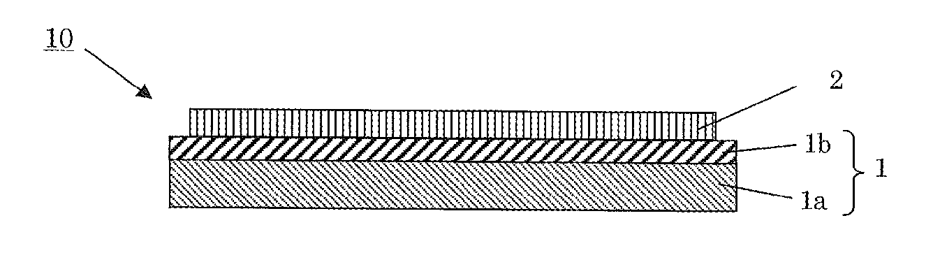
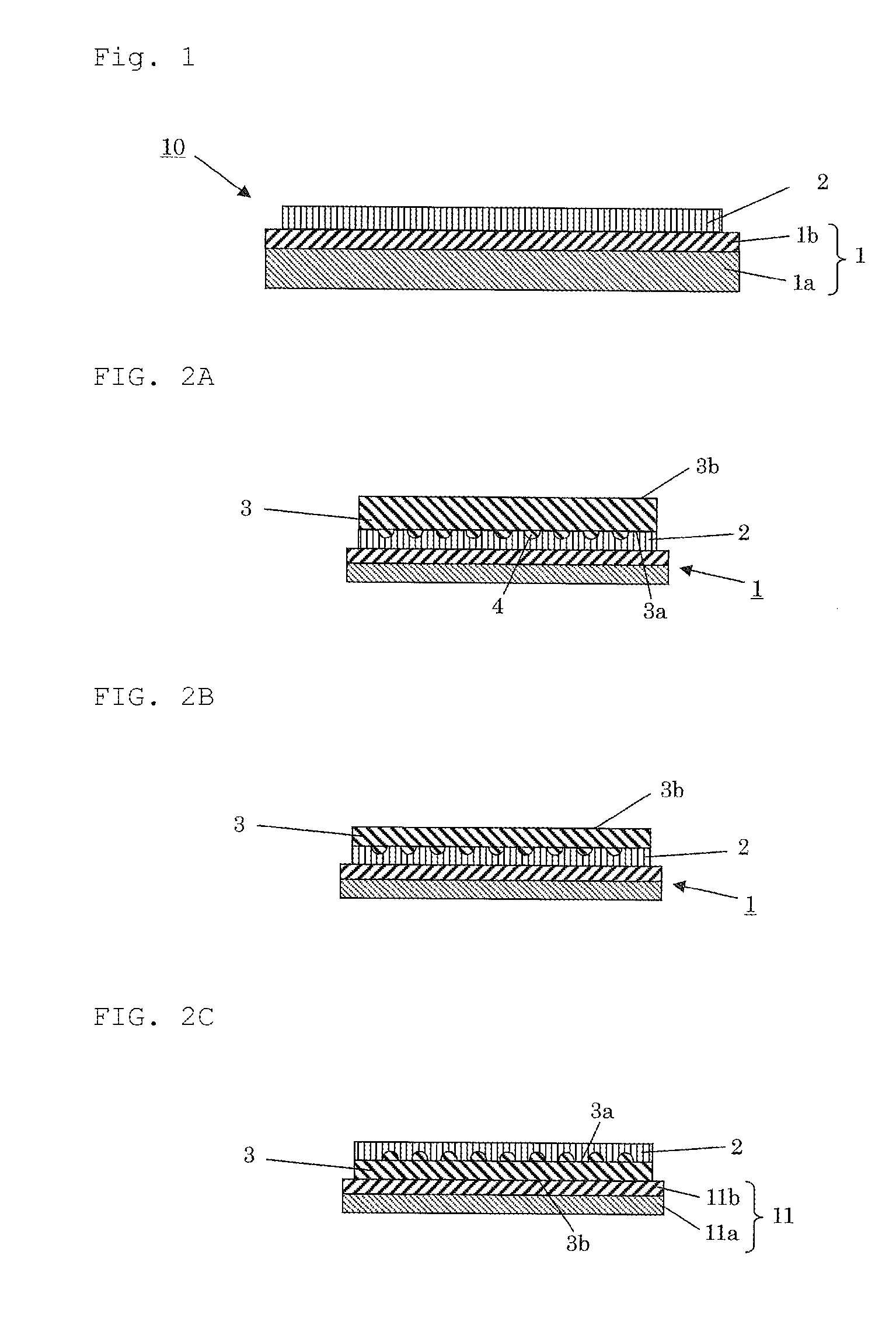
[0037]Hereinafter, one embodiment of the present invention will be described using as an example a sealing sheet with an under-fill material integrated with a backside grinding tape, and a method for producing a semiconductor device using the sealing sheet. Therefore, in this embodiment, a backside grinding tape is used as a pressure-sensitive adhesive tape. Basically, the descriptions below can also be applied to the under-fill material alone.

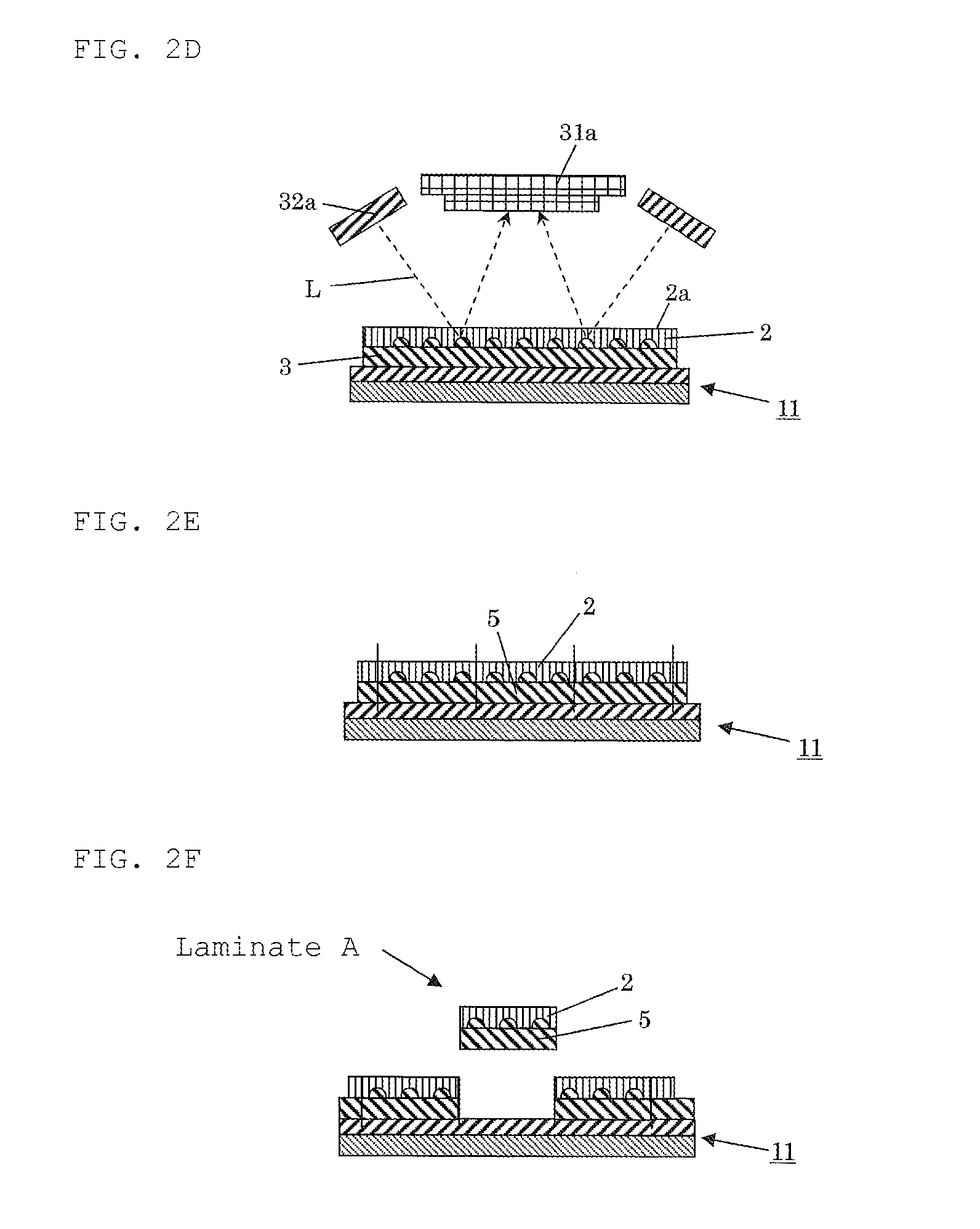
[0038]In this embodiment, backside grinding of a semiconductor wafer is performed using a sealing tape including an under-fill material laminated on a backside grinding tape, followed by performing dicing on a dicing tape and pickup of a semiconductor element, and finally mounting the semiconductor element on an adherend.

[0039]Typical steps in this embodiment include a providing step of providing a sealing sheet including a backside grinding tape and an under-fill material laminated on the backside grinding tape; a bonding step of bonding a ci...

second embodiment

[0164]A semiconductor wafer with a circuit formed on one surface is used in the first embodiment, whereas in this embodiment, a semiconductor device is produced using a semiconductor wafer with circuits formed on both surfaces. Since the semiconductor wafer used in this embodiment has an intended thickness, a grinding step is omitted. Thus, as a sealing sheet in the second embodiment, a sealing sheet including a dicing tape and a predetermined under-fill material laminated on the dicing tape is used. Typical steps prior to a position matching step in the second embodiment include a providing step of providing the sealing sheet, a bonding step of bonding together a semiconductor wafer, in which circuit surfaces each having a connection member are formed on both surfaces thereof, and the under-fill material of the sealing sheet, a dicing step of dicing the semiconductor wafer to form a semiconductor element with the under-fill material, and a pickup step of peeling off the semiconduct...

third embodiment

[0180]In the first embodiment, a back surface grinding tape is used as a constituent member of a sealing sheet, whereas in this embodiment, a pressure-sensitive adhesive layer of the back surface grinding tape is not provided, and a base material alone is used. Thus, a sealing sheet of this embodiment is in such a state that an under-fill material is laminated on a base material. In this embodiment, a grinding step can be optionally carried out, but irradiation of ultraviolet rays before a pickup step is not carried out because a pressure-sensitive adhesive layer is omitted. Except for these aspects, a predetermined semiconductor device can be produced through the same steps as those in the first embodiment.

Other Embodiments

[0181]In the first to third embodiments, dicing using a dicing blade is employed in the dicing step, but in place thereof, so-called stealth dicing may be employed in which a reformed part is formed in a semiconductor wafer by laser irradiation, and the semicond...


PUM

PropertyMeasurementUnit
hazeaaaaaaaaaa
viscosityaaaaaaaaaa
peel strengthaaaaaaaaaa

Abstract

Provided are an under-fill material which is capable of reducing a difference in thermal response behavior between a semiconductor element and an adherend and which makes it easy and convenient to perform alignment for mounting the semiconductor element, a sealing sheet including the under-fill material, and a method for producing a semiconductor device using the under-fill material. In the under-fill material of the present invention, a haze is 70% or less before a heat curing treatment, and a storage elastic modulus E′ [MPa] and a thermal expansion coefficient α [ppm / K] after the under-fill material is subjected to a heat curing treatment at 175° C. for 1 hour satisfy the following formula (1) at 25° C.: 10000<E′×α<250000 [Pa / K].

Description

TECHNICAL FIELD[0001]The present invention relates to an under-fill material, a sealing sheet, and a method for producing a semiconductor device.BACKGROUND ART[0002]In recent years, demands for high-density mounting have been increased as electronic instruments have become smaller and thinner. Accordingly, for semiconductor packages, the surface mount type suitable for high-density mounting has become mainstream, in place of the conventional pin insertion type. In the surface mount type, a lead is soldered directly to a printed board or the like. For a heating method, the whole of a package is heated by infrared reflow, vapor phase reflow, solder dip, or the like to perform mounting.[0003]After surface mounting, a sealing resin is filled in a space between a semiconductor element and a substrate for ensuring protection of the surface of the semiconductor element and connection reliability between the semiconductor element and the substrate. As this sealing resin, a liquid sealing re...

Claims


Application Information

Patent Timeline
Patent Type & Authority Applications(United States)
IPC IPC(8): H01L23/29B32B7/12H01L21/56H01L21/683H01L23/00
CPCH01L23/29H01L21/563H01L21/6836H01L24/81B32B2307/51H01L2221/68327H01L2224/81191B32B2457/14B32B7/12H01L2221/68363H01L2221/68377H01L2221/68381H01L2221/68386H01L24/27H01L2224/14181H01L2224/73104H01L2224/73204H01L2224/83191H01L2924/15787H01L2224/16225H01L2924/351H01L2924/3512C09K3/1006H01L2224/271H01L2224/29318H01L2224/29371H01L2224/29324H01L2224/2939H01L23/3114H01L21/561H01L23/544H01L24/13H01L24/14H01L24/16H01L24/29H01L24/32H01L24/73H01L24/75H01L24/83H01L24/92H01L24/94H01L2223/54426H01L2224/13025H01L2224/13111H01L2224/13144H01L2224/13147H01L2224/16227H01L2224/16245H01L2224/2919H01L2224/2929H01L2224/293H01L2224/29311H01L2224/29316H01L2224/29339H01L2224/29344H01L2224/29347H01L2224/29355H01L2224/29364H01L2224/29387H01L2224/29393H01L2224/32225H01L2224/32245H01L2224/75753H01L2224/81193H01L2224/81204H01L2224/81815H01L2224/83204H01L2224/83862H01L2224/8388H01L2224/92H01L2224/9211H01L2224/94H01L2924/15311H01L2224/27003H01L2224/2744H01L2224/81123H01L2224/83123C09J201/00C09K3/10H01L23/31H01L2221/6834H01L2924/01006H01L2924/00014H01L2924/014H01L2924/01082H01L2924/01047H01L2924/01029H01L2924/0103H01L2924/01083H01L2224/27H01L2224/81H01L2224/83H01L21/304H01L21/78H01L2924/05442H01L2924/00H01L23/293
Inventor MORITA, KOSUKETAKAMOTO, NAOHIDE
Owner NITTO DENKO CORP
Why Eureka
Try Eureka