
Nonvolatile memory device

Active Publication Date: 2016-03-03
SAMSUNG ELECTRONICS CO LTD
View PDF4 Cites 2 Cited by
  • Summary
  • Abstract
  • Description
  • Claims
  • Application Information

AI Technical Summary

Benefits of technology

The invention provides a nonvolatile memory device with multiple memory cells stacked perpendicular to a substrate. The device also includes string select transistors and a bit line. The invention also provides methods for erasing the memory cells by using one directional devices connected between the substrate and the string select lines, or between a pocket well and the string select lines. The technical effects of the invention include a more efficient and efficient method for erasing multiple memory cells simultaneously.

Problems solved by technology

A volatile memory device loses its stored data when its power supply is interrupted.

Method used


Image

  • Nonvolatile memory device
  • Nonvolatile memory device
  • Nonvolatile memory device

Examples


first embodiment

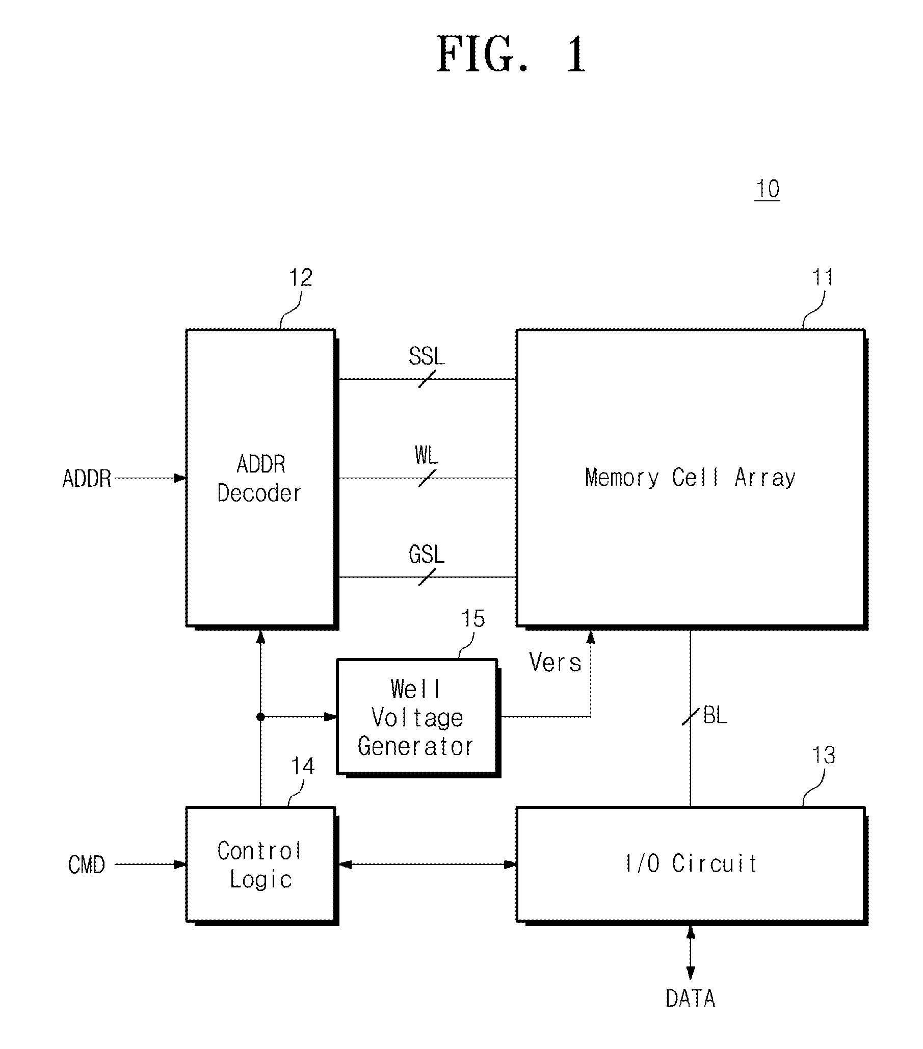
[0066]FIG. 7 is a block diagram illustrating a nonvolatile memory device in accordance with the inventive concept. Referring to FIG. 7, a nonvolatile memory device 100 may include a memory cell array 110, an address decoder 120, an input / output circuit 130, control logic 140 and a well voltage generator 150.

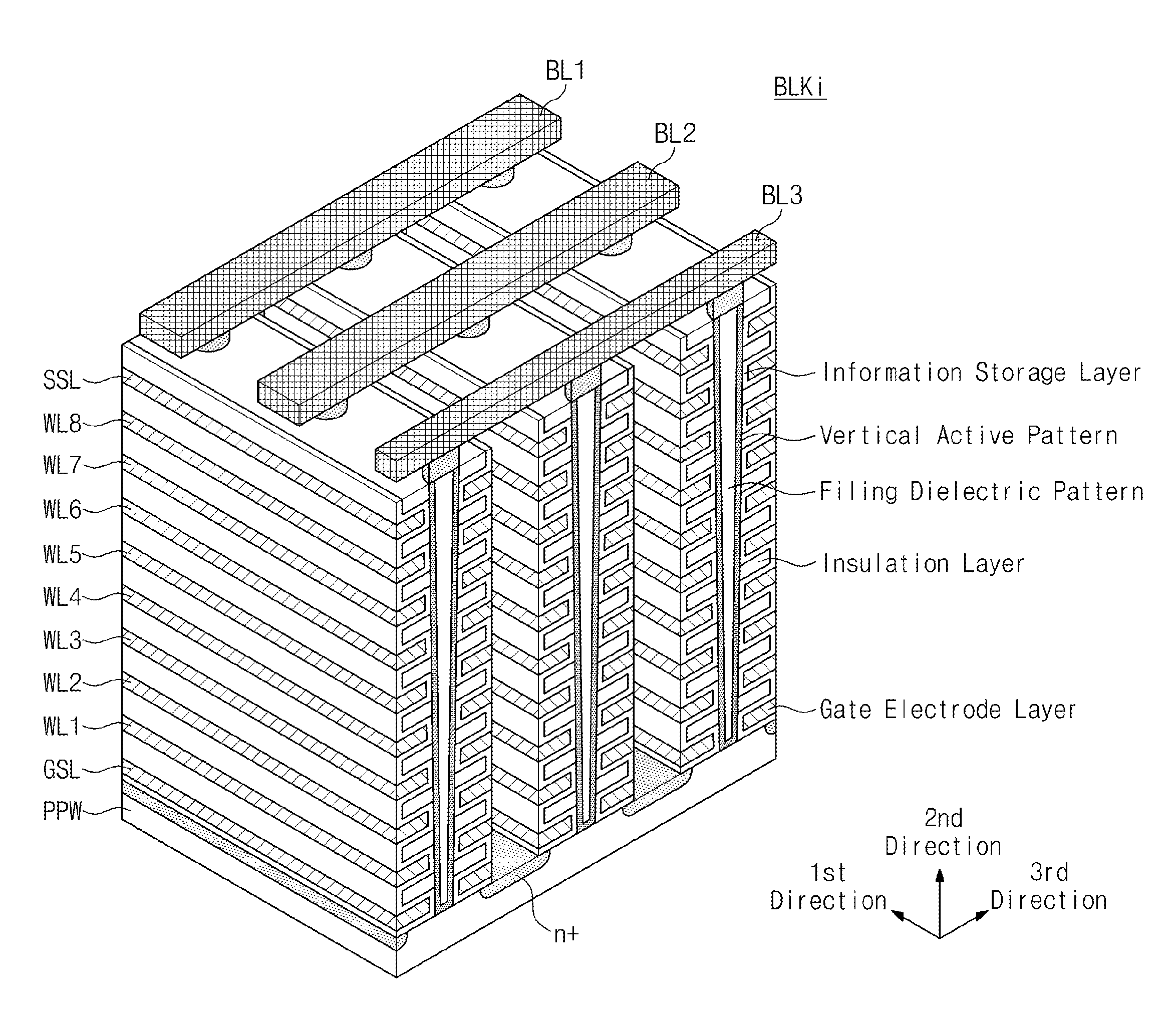
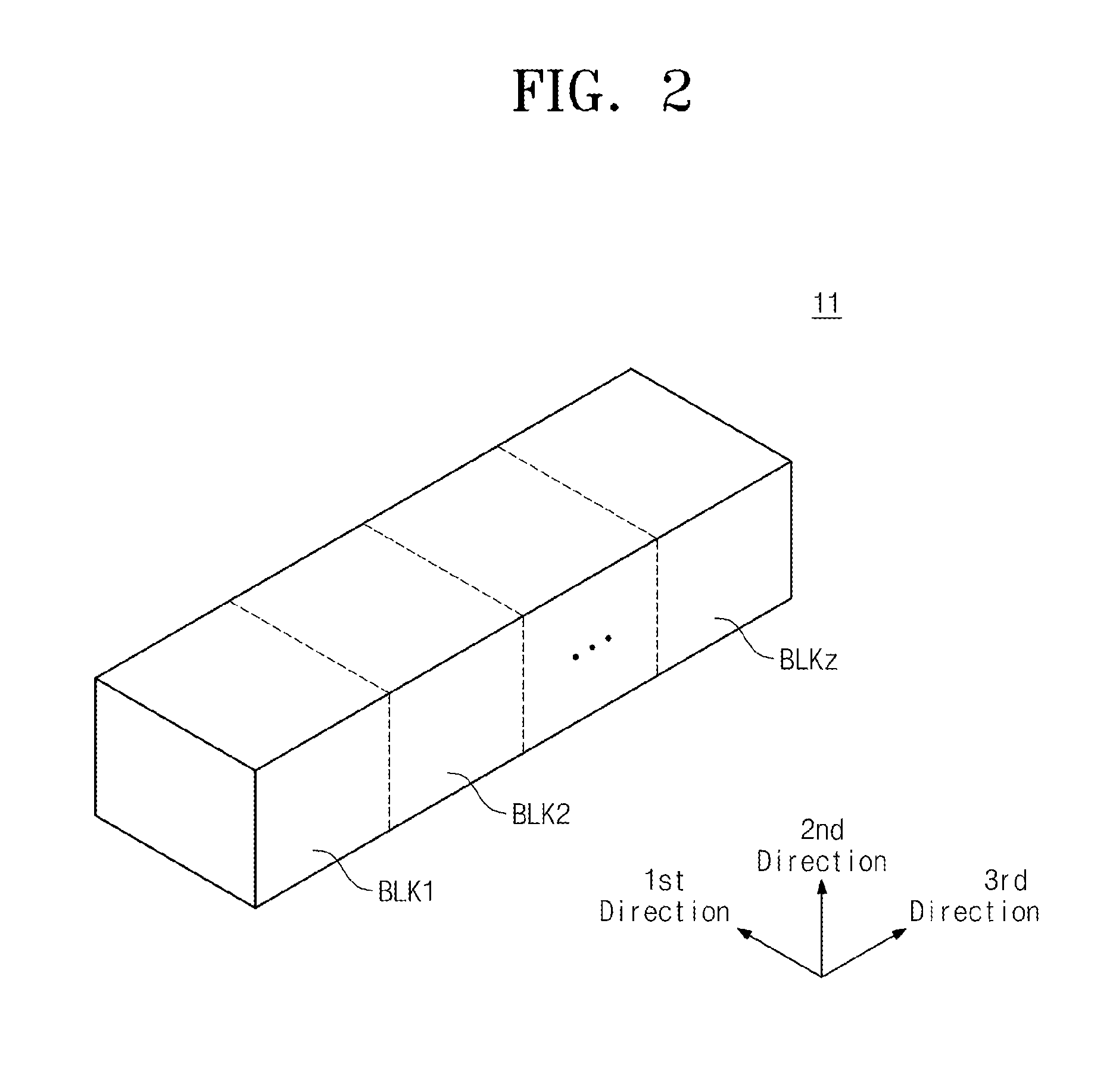
[0067]The memory cell array 110 may be connected to the address decoder 120. The memory cell array 110 may be connected to the input / output circuit 130 through bit lines BL. The memory cell array 110 may include a plurality of memory cells. The memory cells may be stacked on a substrate. For example, a pocket well 111 may be formed on the substrate. The pocket well 111 may be formed of a P-type semiconductor. However, the pocket well 111 is not limited thereto. The memory cells may be stacked on the pocket well 111. Each memory cell can store one or more bits.

[0068]String select lines SSL may be connected to the pocket well 111 through a one directional device 112. The one direct...

second embodiment

[0092]FIG. 12 is a block diagram illustrating a nonvolatile memory device in accordance with the inventive concept. Referring to FIG. 12, a nonvolatile memory device 200 may include a memory cell array 210, an address decoder 220, an input / output circuit 230, control logic 240, and a well voltage generator 250. Since a basic constitution of the nonvolatile memory device 200 is similar or the same as that of the nonvolatile memory device 100 of FIG. 7, a description thereof is omitted.

[0093]The memory cell array 210 may include upper string select transistors 213 and lower string select transistors 216. The upper string select transistors 213 may be connected to the address decoder 220 through upper string select lines SSLu. The lower string select transistors 216 may be connected to the address decoder 220 through lower string select lines SSLd.

[0094]The memory cell array 210 may include a first pocket well 211 and a second pocket well 214. The first pocket well 211 and the second p...

third embodiment

[0121]FIG. 18 is a block diagram illustrating a nonvolatile memory device in accordance with the inventive concept. Referring to FIG. 18, a nonvolatile memory device 300 may include a memory cell array 310, an address decoder 320, an input / output circuit 330, control logic 340, and a well voltage generator 350. Since a basic constitution of the nonvolatile memory device 300 is similar or the same as that of the nonvolatile memory device 100 of FIG. 7, a description thereof is omitted.

[0122]The memory cell array 300 may include upper string select transistors 313 and lower string select transistors 316. The upper string select transistors 313 may be connected to the address decoder 320 through upper string select lines SSLu. The lower string select transistors 316 may be connected to the address decoder 320 through lower string select lines SSLd.

[0123]The upper and lower string select lines SSLu and SSLd may be connected to a pocket well 311 through a one directional device 312. The ...


PUM


Abstract

The nonvolatile memory device includes a plurality of memory cells being stacked in a direction perpendicular to a substrate. A string select transistor is connected between the memory cells and a bit line. A string select line is connected to the string select transistor. A one directional device is connected between the substrate and the string select line and configured to transmit a bias voltage from the substrate toward the string select line in an erase operation.

Description

CROSS-REFERENCE TO RELATED APPLICATIONS[0001]This U.S. non-provisional patent application claims priority under 35 U.S.C. §119 to Korean Patent Application No. 10-2014-0115313, filed on Sep. 1, 2014, the entire contents of which are hereby incorporated by reference.BACKGROUND OF THE INVENTION[0002]The inventive concept relates to semiconductor memories, and more particularly, to a nonvolatile memory device.[0003]A semiconductor memory device is a memory device which is embodied using a semiconductor such as silicon Si, germanium Ge, gallium arsenide GaAs, indium phosphide InP, etc. A semiconductor memory device may be classified into a volatile semiconductor memory device or a nonvolatile semiconductor memory device.[0004]A volatile memory device loses its stored data when its power supply is interrupted. Examples of the a volatile memory device include a static RAM (SRAM), a dynamic RAM (DRAM), a synchronous DRAM (SDRAM), etc. A nonvolatile memory device retains its stored data eve...

Claims


Application Information

Patent Timeline
IPC IPC(8): H01L27/115
CPCH01L27/11582H01L27/1157G11C16/14G11C16/3427H10B43/50H10B43/27H10B43/35
Inventor NAM, SANG-WAN
Owner SAMSUNG ELECTRONICS CO LTD
Features
  • Generate Ideas
  • Intellectual Property
  • Life Sciences
  • Materials
  • Tech Scout
  • Unparalleled Data Quality
  • Higher Quality Content
  • 60% Fewer Hallucinations
Learn More