Insulated gate type switching device

a switching device and gate type technology, applied in the field of insulated gate type switching devices, can solve the problems of increasing difficulty in forming the channel in the body region, and the difficulty of the channel to be formed in the body region to raise so as to increase the amount of mobile electrons, and reduce the resistance of the channel

Inactive Publication Date: 2016-03-03
TOYOTA JIDOSHA KK
View PDF0 Cites 13 Cited by
  • Summary
  • Abstract
  • Description
  • Claims
  • Application Information

AI Technical Summary

Benefits of technology

[0008]In this insulated gate type switching device, raising a gate voltage to a potential substantially equal to the theoretical threshold level of the second body region forms a channel in the second body region. Since the theoretical threshold level of the first body region is higher than the theoretical threshold level of the second body region, the insulated gate type switching device is not turned on at this stage. Further raising the gate voltage to a potential substantially equal to the theoretical threshold level of the first body region forms a channel in the first body region. At this stage, the first region and the second region are connected to each other via the channel, so that the insulated gate type switching device is turned on. Therefore, a gate threshold level of this insulated gate type switching device is determined on the basis of the high theoretical threshold level of the first body region. Further, a rise in the gate voltage to the theoretical threshold level of the first body region increases amount of mobile electrons in the channel formed in the second body region. For this reason, the resistance of the channel that is formed in the second body region is low. This allows a reduction in the resistance of the channel. In this way, the structure of this insulated gate type switching device can achieve a high gate threshold level and a low channel resistance.

Problems solved by technology

On the other hand, making it difficult for the channel to be formed in the body region raises resistance of the channel.
For this reason, there has conventionally been such a problem that making the gate threshold level higher raises the channel resistance.

Method used


Image

  • Insulated gate type switching device
  • Insulated gate type switching device
  • Insulated gate type switching device

Examples


embodiment 1

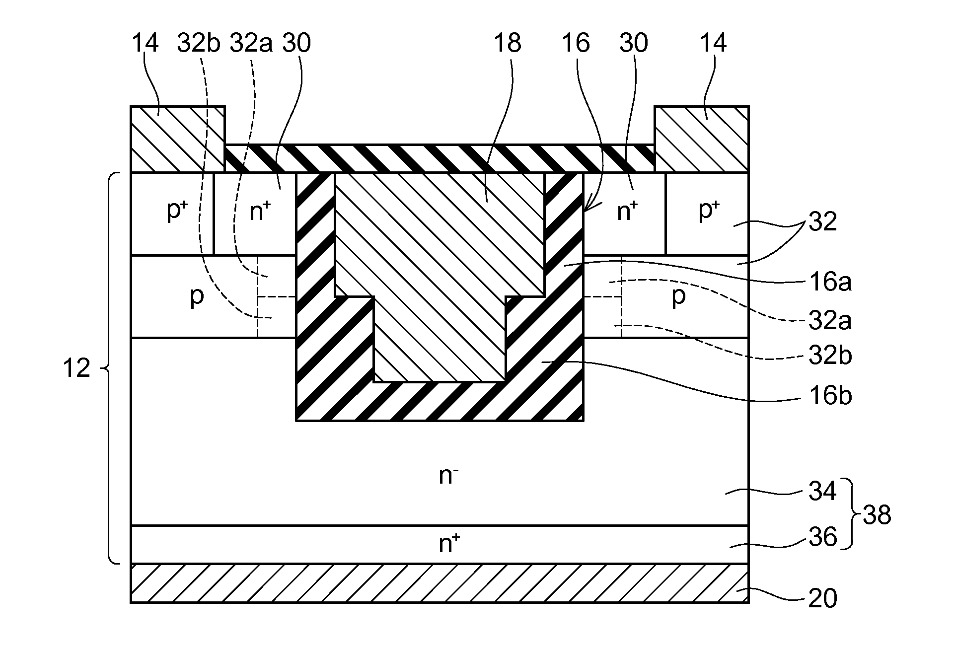
[0016]FIG. 1 shows a MOSFET 10. The MOSFET 10 includes a semiconductor substrate 12. The semiconductor substrate 12 is made of SiC.

[0017]A plurality of source electrodes 14 is formed on an upper surface of the semiconductor substrate 12. The source electrodes 14 are formed with a clearance between each other. Each of the source electrodes 14 is in contact with the upper surface of the semiconductor substrate 12.

[0018]A gate insulating film 16 is formed on the upper surface of the semiconductor substrate 12. The gate insulating film 16 is formed between two source electrodes 14. The source electrodes 14 are in contact with the upper surface of the semiconductor substrate 12. The gate insulating film 16 is made of SiO2. The gate insulating film 16 includes a thin film portion 16a and a thick film portion 16b. The thin film portion 16a is small in thickness, and the thick film portion 16b is large in thickness. The thick film portion 16b is formed in an intermediate position between th...

embodiment 2

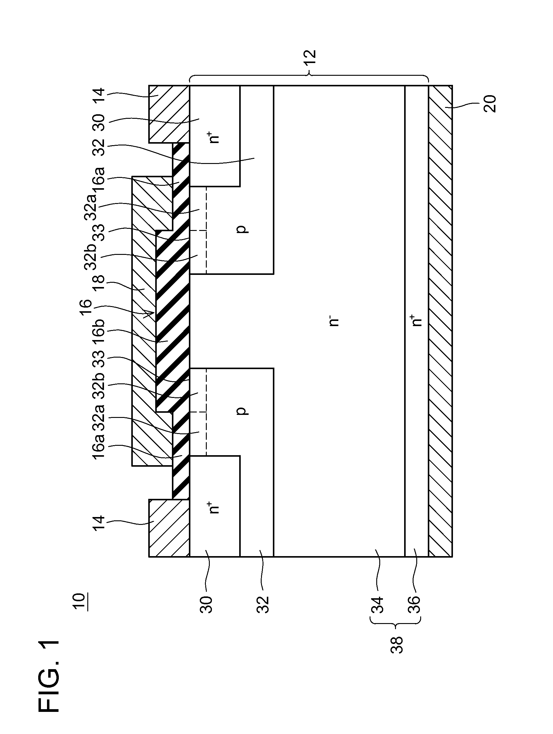
[0036]FIG. 2 shows a MOSFET 200 of Embodiment 2. The MOSFET 200 of Embodiment 2 is different in its configuration of the gate insulating film 16 from the MOSFET 10 of Embodiment 1, and is identical in other configurations to the MOSFET 10 of Embodiment 1. In the MOSFET 200 of Embodiment 2, the thickness of the gate insulating film 16 is constant. Further, in the MOSFET 200 of Embodiment 2, the gate insulating film 16 includes an insulating film 16c made of HfO2 and an insulating film 16d made of SiO2. The insulating film 16c (i.e. HfO2) has a relative dielectric constant ∈r of about 30, and the insulating film 16d (i.e. SiO2) has a relative dielectric constant ∈r of about 3.9. Therefore, a dielectric constant ∈ (=∈r∈0, where ∈0 is the dielectric constant of a vacuum) of the insulating film 16c is larger than a dielectric constant ∈ (=∈r∈0) of the insulating film 16d. The insulating film 16c is formed in an area corresponding to the thin film portion 16a of Embodiment 1, and the insu...

embodiment 3

[0043]FIG. 3 shows a MOSFET 300 of Embodiment 3. The MOSFET 300 of Embodiment 3 is different in its configuration of the gate insulating film 16 from the MOSFET 10 of Embodiment 1, and is identical in other configurations to the MOSFET of Embodiment 1. In the MOSFET 300 of Embodiment 3, the thin film portion 16a is made of SiO2, and the thick film portion 16b is made of HfO2.

[0044]The following discusses the theoretical threshold level Vth of the source-side body regions 32a and that of the drain-side body regions 32b. For the same reasons as those noted in Embodiment 1, the source-side body regions 32a and the drain-side body regions 32b are equal in φMS and φFB to each other. Further, for the same reason as that noted in Embodiment 2, the source-side body regions 32a and the drain-side body regions 32b are equal in value QB to each other.

[0045]A thickness d1 of the thin film portion 16a on the source-side body regions 32a is smaller than a thickness d2 of the thick film portion 16...


PUM


Abstract

An insulated gate type switching device includes: a first region being of a first conductivity type; a body region being of a second conductivity type and in contact with the first region; a second region being of the first conductivity type and separated from the first region by the body region; an insulating film being in contact with the first region, the body region and the second region; and a gate electrode facing the body region via the insulating film. The body region includes a first body region and a second body region. The first body region has a theoretical threshold level Vth larger than that of the second body region.

Description

CROSS-REFERENCE TO RELATED APPLICATION[0001]This application claims priority to Japanese Patent Application No. 2014-178896 filed on Sep. 3, 2014, the contents of which are hereby incorporated by reference into the present application.TECHNICAL FIELD[0002]A technology disclosed herein relates to an insulated gate type switching device.BACKGROUND ART[0003]Japanese Patent Application Publication No. 2009-158788 discloses a MOSFET.[0004]The application of a voltage equal to or higher than a threshold level to a gate electrode forms a channel in a body region, so that the MOSFET is turned on.BRIEF SUMMARY[0005]A gate threshold level of an insulated gate type switching device can be controlled by structures and materials of a body region, a gate insulating film, and a gate electrode. The gate threshold level can be made higher by making it difficult for a channel to be formed in the body region. On the other hand, making it difficult for the channel to be formed in the body region raises...

Claims


Application Information

Patent Timeline
Patent Type & Authority Applications(United States)
IPC IPC(8): H01L29/78H01L29/08H01L29/10H01L29/739
CPCH01L29/7813H01L29/7397H01L29/0882H01L29/0865H01L29/1095H01L29/1045H01L29/1608H01L29/42368H01L29/4983H01L29/512H01L29/7802
Inventor SUGIMOTO, MASAHIROKUTSUKI, KATSUHIROAOI, SACHIKOWATANABE, YUKIHIKOEBIHARA, YASUHIRO
Owner TOYOTA JIDOSHA KK
Why Eureka
Try Eureka