Method and apparatus for providing multi-page read and write using SRAM and nonvolatile memory devices

a nonvolatile memory and multi-page read and write technology, applied in the field of memory and storage devices, can solve the problems of a relative long time to transfer data from sram to an slow programming and/or erasing speed in a nonvolatile memory storage becomes a limitation and/or drawback, and the relative long time to transfer data from sram to the off-chip nvm memory devi

Active Publication Date: 2016-03-17
NEO SEMICON
View PDF7 Cites 24 Cited by
  • Summary
  • Abstract
  • Description
  • Claims
  • Application Information

AI Technical Summary

Problems solved by technology

A problem, however, associated with conventional NVM based flash memory is that it has a relatively slow programming speed.
For some applications, a slow programming and / or erasing speed in a nonvolatile memory storage becomes a limitation and / or drawback.
Another drawback associated with NVM is that it takes a relative long time to transfer data from SRAM to an off-chip NVM memory device.

Method used


Image

  • Method and apparatus for providing multi-page read and write using SRAM and nonvolatile memory devices
  • Method and apparatus for providing multi-page read and write using SRAM and nonvolatile memory devices
  • Method and apparatus for providing multi-page read and write using SRAM and nonvolatile memory devices

Examples


Embodiment Construction

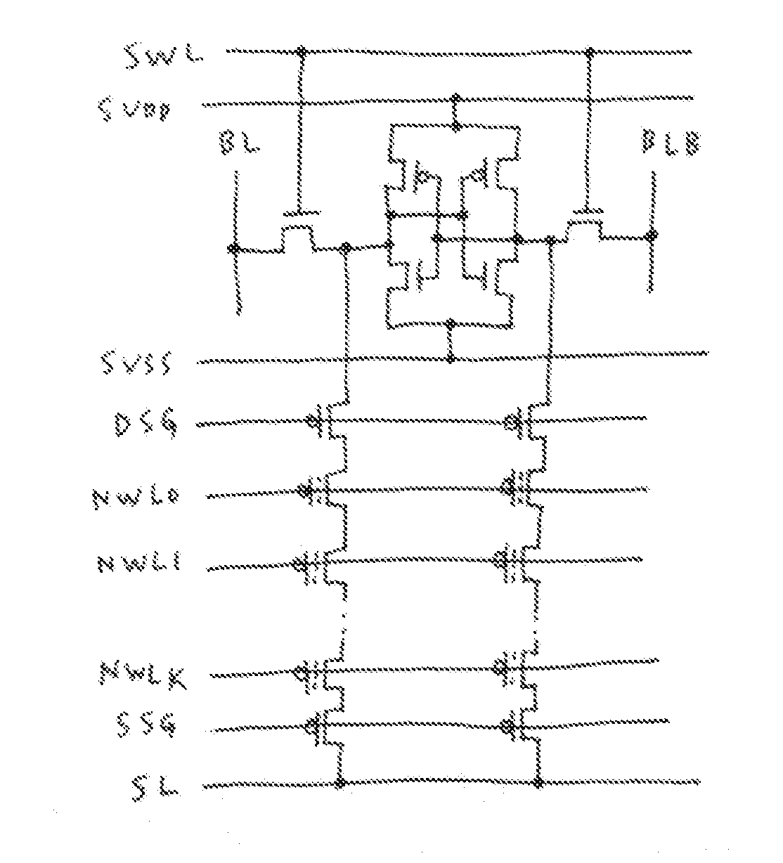
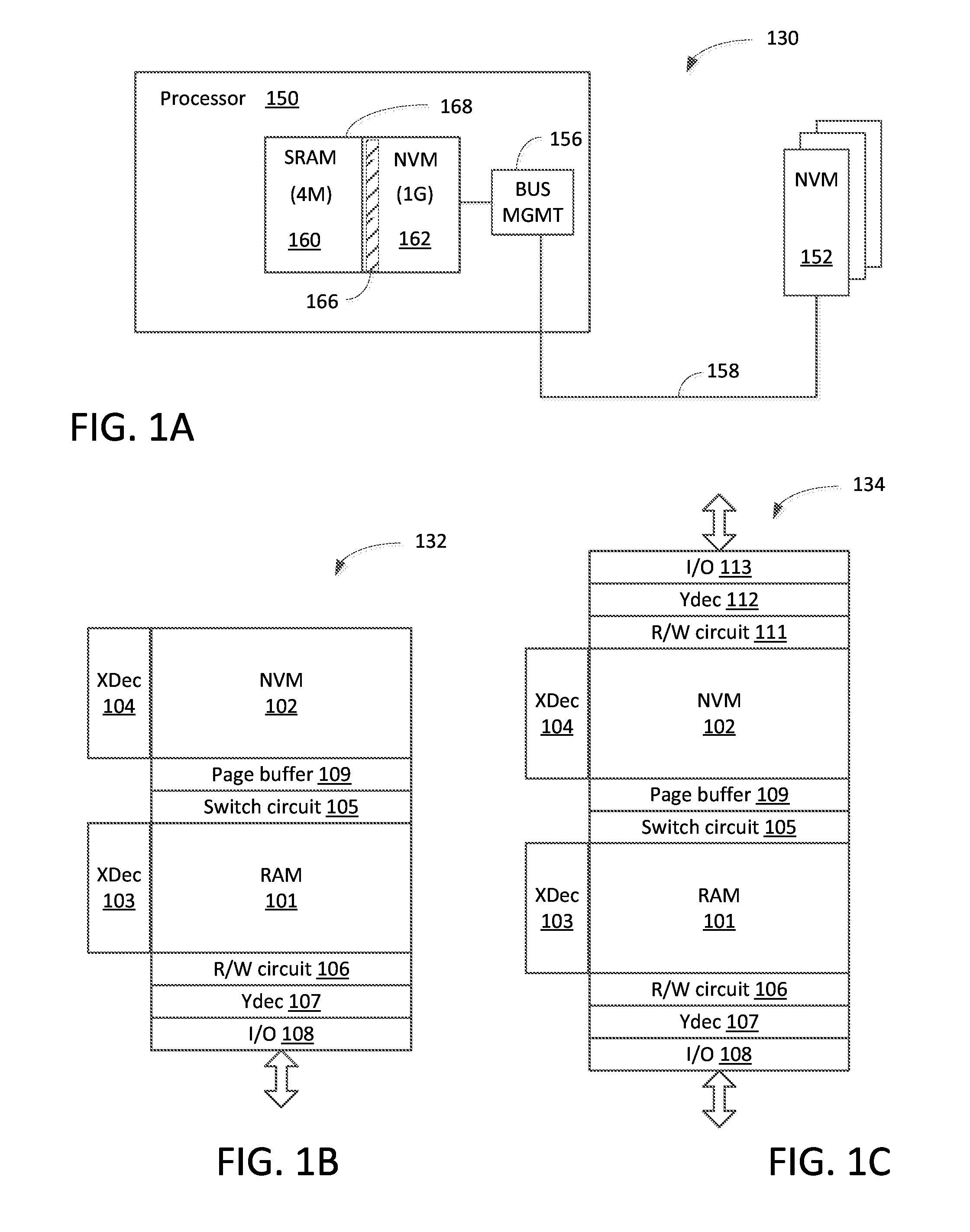
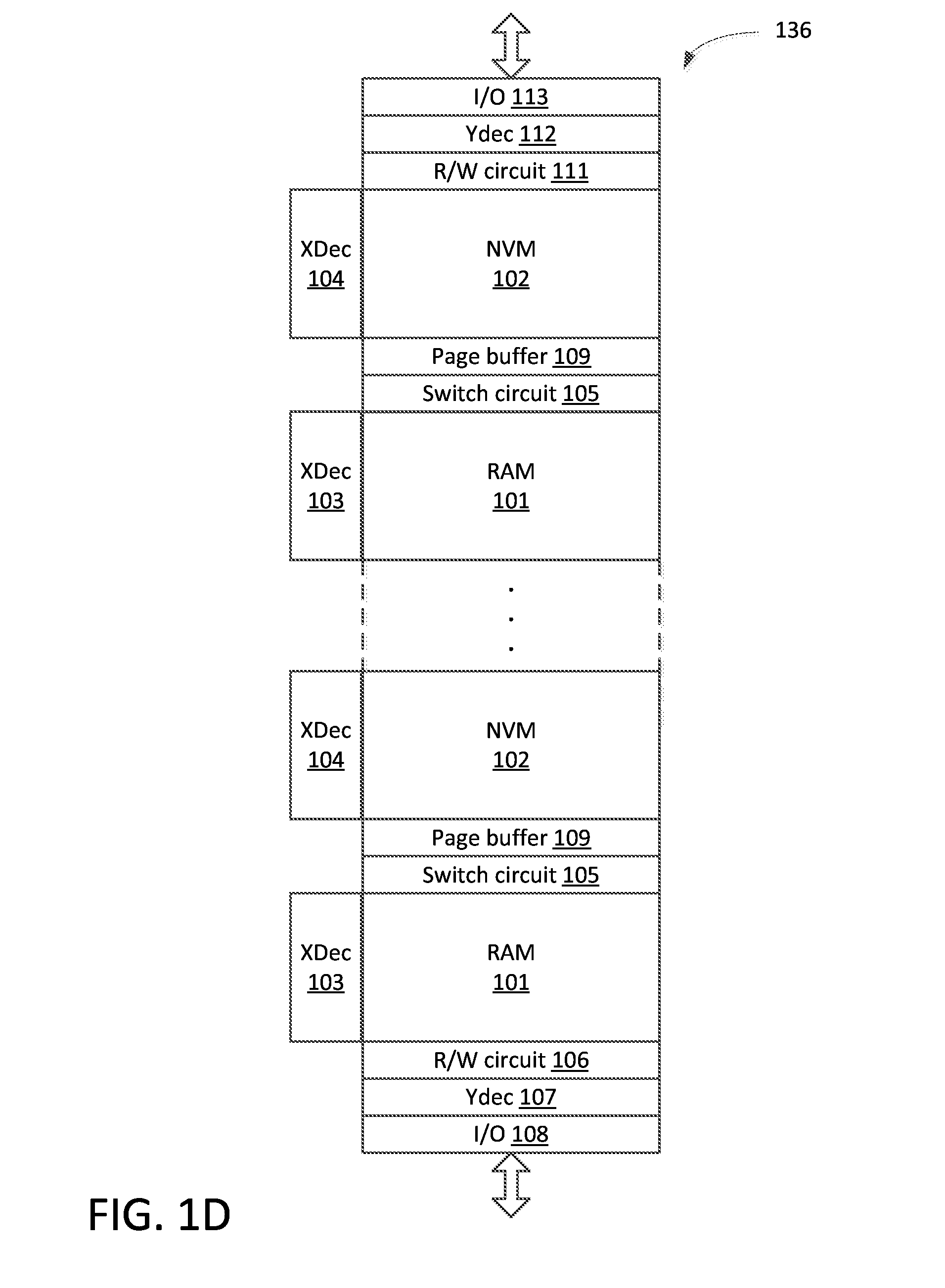
[0024]Exemplary embodiment(s) of the present invention is described herein in the context of a method, device, and apparatus for improving nonvolatile memory writing speed using multiple-page programming.

[0025]Those of ordinary skilled in the art will realize that the following detailed description of the present invention is illustrative only and is not intended to be in any way limiting. Other embodiments of the present invention will readily suggest themselves to such skilled persons having the benefit of this disclosure. Reference will now be made in detail to implementations of the exemplary embodiments of the present invention as illustrated in the accompanying drawings. The same reference indicators (or numbers) will be used throughout the drawings and the following detailed description to refer to the same or like parts.

[0026]In accordance with the embodiment(s) of present invention, the components, process steps, and / or data structures described herein may be implemented us...


PUM


Abstract

A memory device includes a static random-access memory (“SRAM”) circuit and a first nonvolatile memory (“NVM”) string, a second NVM string, a first and a second drain select gates (“DSGs”). The SRAM circuit is able to temporarily store information in response to bit line (“BL”) information which is coupled to at the input terminal of the SRAM circuit. The first NVM string having at least one nonvolatile memory cell is coupled to the output terminal of the SRAM. The first DSG is operable to control the timing for storing information at the output terminal of the SRAM to the first nonvolatile memory. The second NVM string having at least one nonvolatile memory cell is coupled to the output terminal of the SRAM. The second DSG controls the timing for storing information at the output terminal of the SRAM to the second nonvolatile memory string.

Description

PRIORITY[0001]This application claims the benefit of priority based upon U.S. Provisional Patent Application Ser. No. 62 / 050,755, filed on Sep. 15, 2014 and entitled “Novel Memory Array Combining RAM, NVM, and NVRAM,” and U.S. Provisional Patent Application Ser. No. 62 / 062,909, filed on Oct. 12, 2014 and entitled “NVSRAM with SRAM and NAND Cells Structure,” all of which are hereby incorporated herein by reference in their entireties.FIELD OF THE INVENTION[0002]The exemplary embodiment(s) of the present invention relates to the field of semiconductor and integrated circuits. More specifically, the exemplary embodiment(s) of the present invention relates to memory and storage devices.BACKGROUND OF THE INVENTION[0003]Nonvolatile memory (“NVM”), such as NAND or NOR based flash memory, is widely used in today's technology world. Its unique cell and array structure provide a small cell size, high density, low write current, and higher data throughout. NVM such as NAND based flash memory b...

Claims


Application Information

Patent Timeline
Patent Type & Authority Applications(United States)
IPC IPC(8): G11C14/00G11C11/419G11C16/04G11C16/10
CPCG11C14/0063G11C11/419G11C16/0483G11C16/10G11C11/005
Inventor HSU, FU-CHANG
Owner NEO SEMICON
Why Eureka
Try Eureka