Supercharge Your Innovation With Domain-Expert AI Agents!

Precision, high voltage, low power differential input stage with static and dynamic gate protection

Active Publication Date: 2016-03-17
FONDERIE MAARTEN JEROEN
View PDF3 Cites 3 Cited by
  • Summary
  • Abstract
  • Description
  • Claims
  • Application Information

AI Technical Summary

Benefits of technology

The patent describes a differential input stage that includes two input circuits that convert a difference in input voltage into an output. The output can be a current or voltage, and can be either singular or differential. Each input circuit has three transistors, a current source, and a resistor. One of the transistors has current terminals connected to the input node and the intermediate node, while the other two transistors are connected in a cascode configuration. The upper cascode transistors are lower voltage transistors, but have high enough threshold voltage to match each other. The input stages also have capacitors to form a low pass filter and additional protection transistors or diodes. The patent also describes an amplifying device that includes this differential input stage. The technical effect is a more symmetrical and efficient conversion of differential input voltage to output with reduced distortion and noise.

Problems solved by technology

Lateral bipolar PNP transistors, however, are relatively slow, and separate ESD circuits are required to protect the inputs.
Furthermore, the base current of a lateral bipolar PNP transistor shows up as input bias current, so that it is generally not suitable for low power applications.
Moreover, high voltage lateral bipolar transistors are not commonly available in modern integrated circuit (IC) process manufacturing technologies.
But such configurations lack the DC precision that is achievable with bipolar designs.
This is the result of the inherent poor matching of high voltage MOSFET transistors.
Also, amplifier circuits built with high-voltage MOSFETs conventionally require gate protection circuits that further decrease the accuracy of the input stages.

Method used


Image

  • Precision, high voltage, low power differential input stage with static and dynamic gate protection
  • Precision, high voltage, low power differential input stage with static and dynamic gate protection
  • Precision, high voltage, low power differential input stage with static and dynamic gate protection

Examples


Embodiment Construction

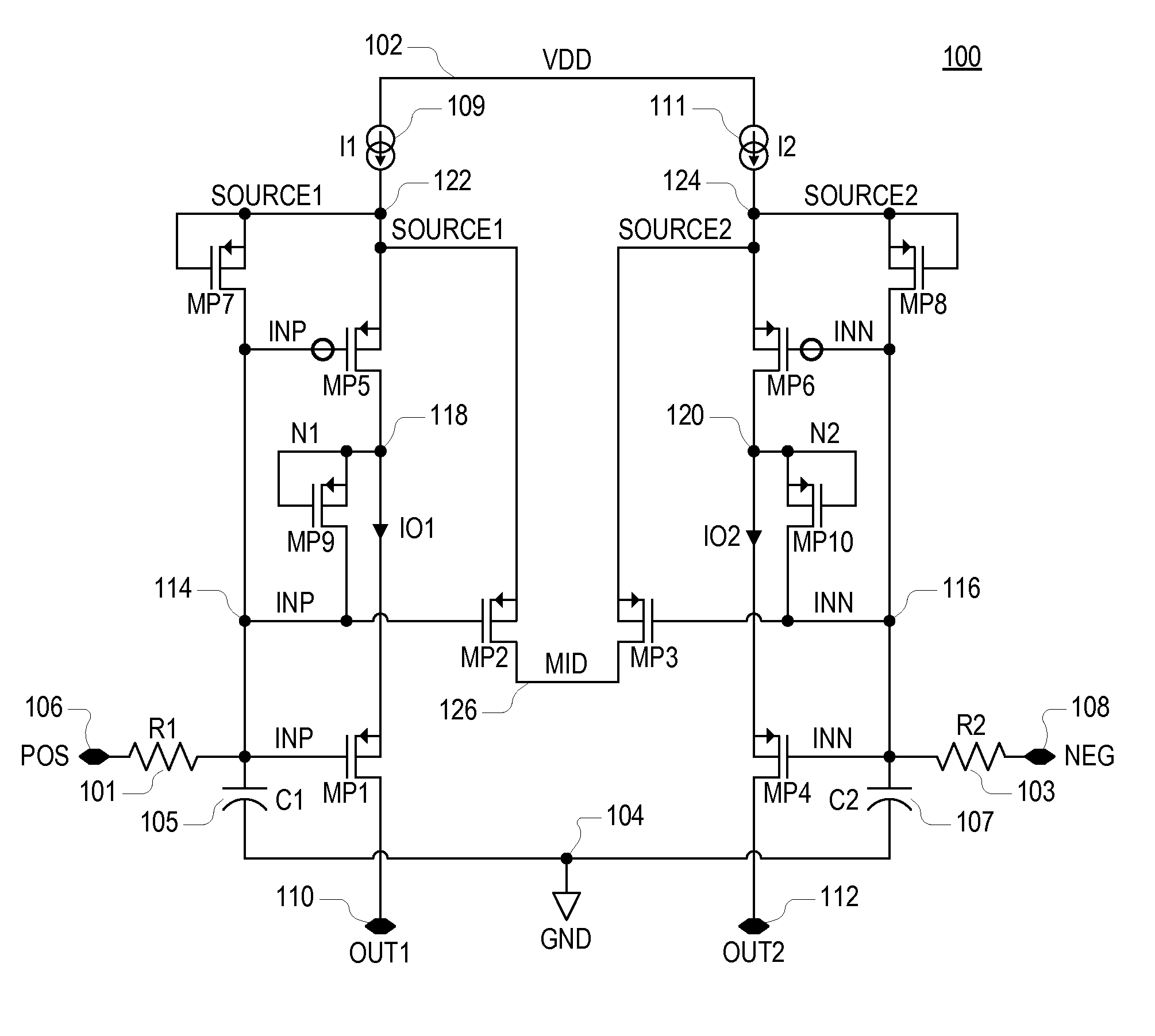
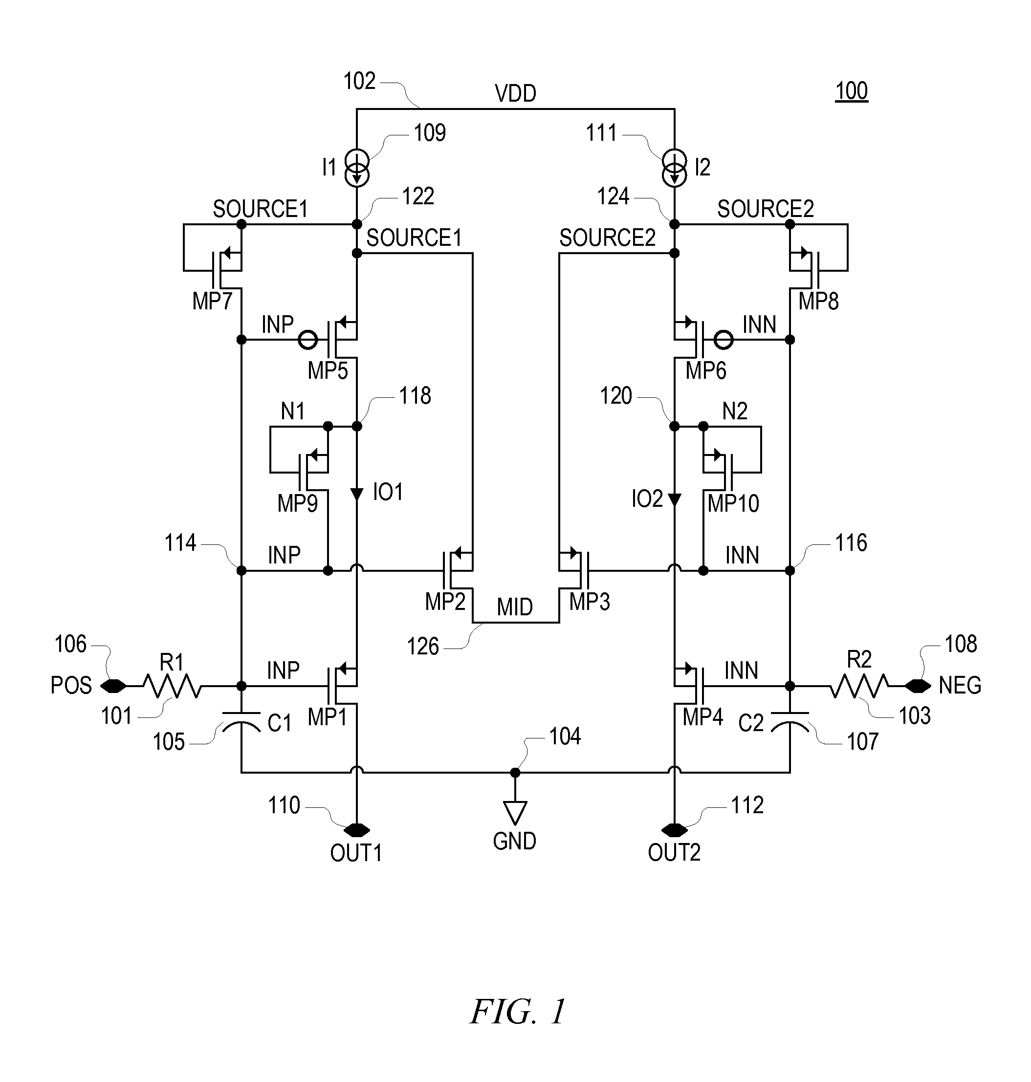
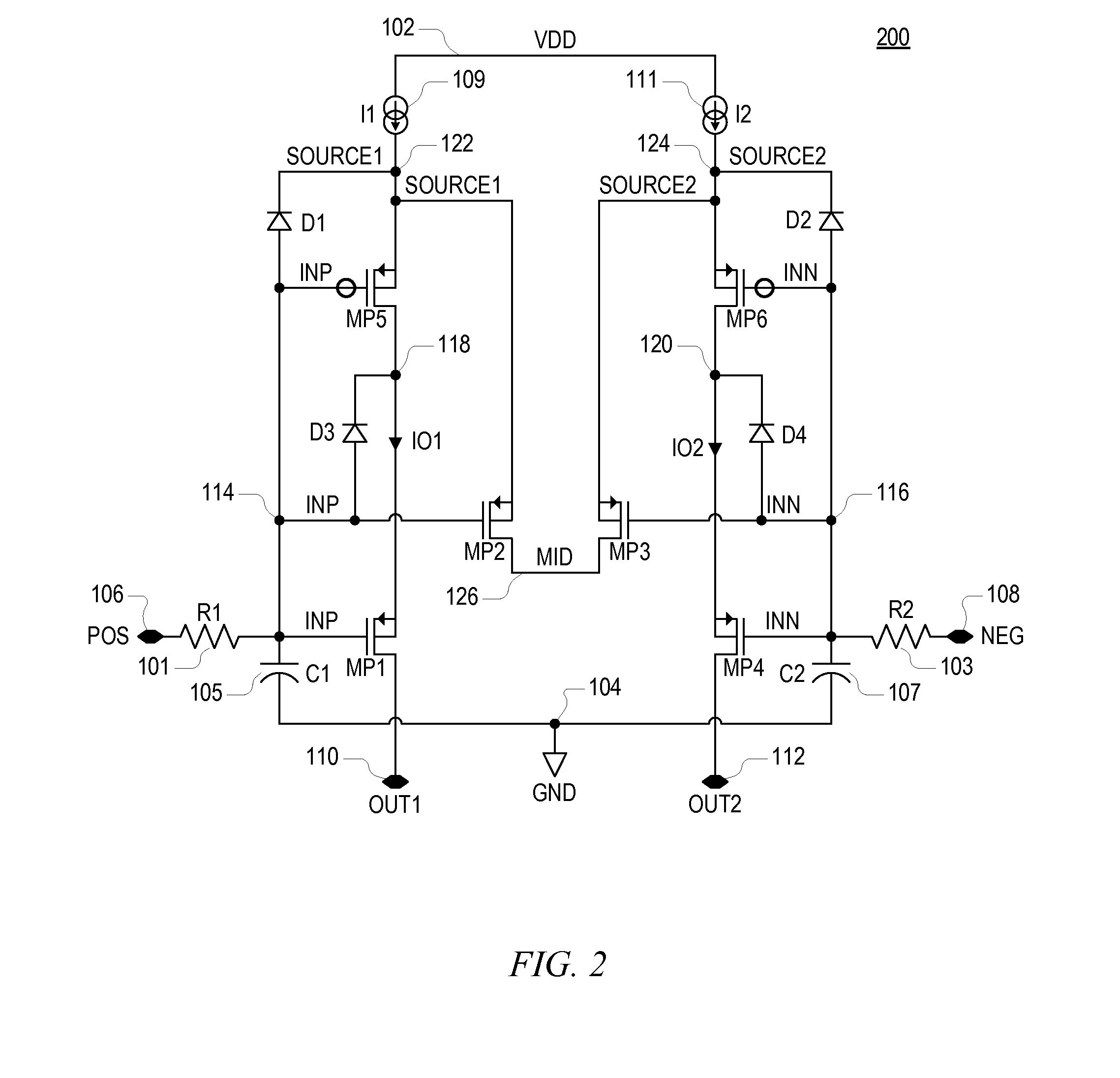
[0016]The present invention uses an improved design that incorporates the performance of low voltage MOSFETs with the high voltage capability of high voltage MOSFETs. In addition, gate protection is provided for the transistors to protect against large DC voltage differences, sudden large signal AC transients, and ESD pulses.

[0017]Embodiments described herein use a cascode combination of a low voltage MOSFET and a high voltage MOSFET. The gates of the low and high voltage MOSFETs are connected to each other to avoid increasing the complexity of, and to avoid degrading the performance of, the resulting circuit. Furthermore, the low voltage MOSFET is fabricated with a gate threshold voltage that is at least as high or higher than that of the high voltage MOSFET. In general, high voltage MOSFETs have higher gate threshold voltages than low voltage MOSFETs. A high threshold, low voltage MOSFET is added to the IC process manufacturing technology and used in the configuration.

[0018]Embodi...


PUM


Abstract

A precision, high voltage, low power differential input stage including static and dynamic gate protection is disclosed herein. The differential input stage incorporates the performance of low voltage transistors with the high voltage capability of high voltage transistors. The transistors may be MOSFETs or the like. In addition, gate protection is provided to protect against large DC voltages and AC voltage transitions. The differential input stage includes a pair of input circuits, such as positive and negative input circuits, each including a cascode combination of low and high voltage transistors. In each cascode stage, the low voltage transistor is fabricated with a gate threshold voltage that is as high or higher than that of the high voltage transistors. The low voltage, high threshold transistors in the cascode stages may be configured to match each other. Resistors and capacitors may be provided to protect against excessive input current and voltage.

Description

CROSS-REFERENCE TO RELATED APPLICATIONS[0001]This application claims the benefit of U.S. Provisional Application Ser. No. 62 / 050,454, filed on Sep. 15, 2014, which is hereby incorporated by reference in its entirety for all intents and purposes.BACKGROUND OF THE INVENTION[0002]1. Field of the Invention[0003]The present invention relates in general to differential input stages, and more particularly to a precision, low power, high voltage differential input stage, with incorporated protection against DC and fast AC transient signals at the input.[0004]2. Description of the Related Art[0005]It is desired to provide a precision, high voltage, low power input stage for analog amplifiers and comparators. Also, it is desired to provide gate protection for the transistors for large direct-current (DC) voltage differences, sudden large signal alternating-current (AC) transients, and protection against electrostatic discharge (ESD) pulses for both powered and unpowered circuits.[0006]It is p...

Claims


Application Information

Patent Timeline
IPC IPC(8): H03F3/45H03F1/52H03F1/56
CPCH03F3/45179H03F2203/45154H03F1/56H03F1/523H03F3/45H03F3/45475H03F2200/444H03F2203/30063H03F2203/45326H03F2203/45352H03F2203/45366
Inventor SCHAFFER, GREGORY LFONDERIE, MAARTEN JEROEN
Owner FONDERIE MAARTEN JEROEN
Features
  • R&D
  • Intellectual Property
  • Life Sciences
  • Materials
  • Tech Scout
  • Unparalleled Data Quality
  • Higher Quality Content
  • 60% Fewer Hallucinations
Learn More