
Liquid crystal display device

a liquid crystal display and display device technology, applied in the field of liquid crystal display devices, can solve the problems of reducing the yield rate of a manufacturing process, reducing the aperture ratio, and reducing the performance of liquid crystal, so as to overcome the problem of color deviation and improve light transmittance and light extraction efficiency

Inactive Publication Date: 2016-03-31
SHENZHEN CHINA STAR OPTOELECTRONICS TECH CO LTD
View PDF5 Cites 7 Cited by
  • Summary
  • Abstract
  • Description
  • Claims
  • Application Information

AI Technical Summary

Benefits of technology

The present invention provides a liquid crystal display device that improves light transmittance and overcomes the issue of color deviation at a large view angle. The device includes a view angle diffusion film, a reflective polarizing beam splitter, and a metallic grating reflector plate. These arrangements separate polarized lights and convert them, resulting in improved light utilization and increased light extraction. Overall, the device provides better light transmission and is more efficient in displaying pictures.

Problems solved by technology

Using ITO electrode of the eight-domain pattern would lead to a reduction of the yield rate of a manufacturing process, a reduction of the aperture ratio, a reduction of liquid crystal performance, and a reduction of light transmittance, and thus the cost of the backlight module is indirectly increased.
On the other hand, using a two-domain or one-domain VA mode solution allows for a signification increase of light transmittance, but color deviation becomes apparently severe at large view angles.
Since the light transmittance of the liquid crystal panel at a large view angle is reduced, the light extraction performance of the backlight module gets deteriorated and the large view angle color deviation issue of the liquid crystal panel is made apparently identifiable.

Method used


Image

  • Liquid crystal display device
  • Liquid crystal display device
  • Liquid crystal display device

Examples


Embodiment Construction

[0029]To further expound the technical solution adopted in the present invention and the advantages thereof, a detailed description is given to a preferred embodiment of the present invention and the attached drawings.

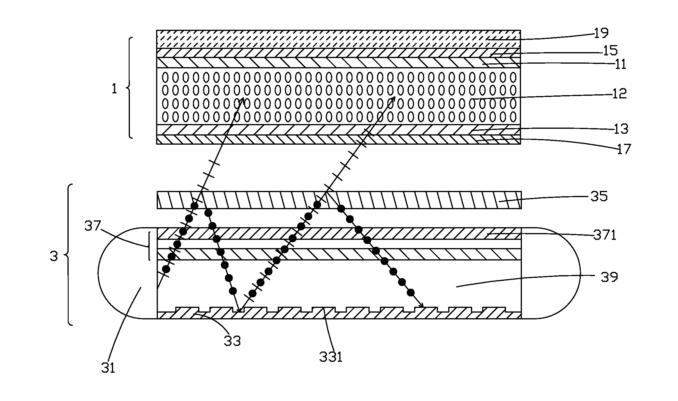
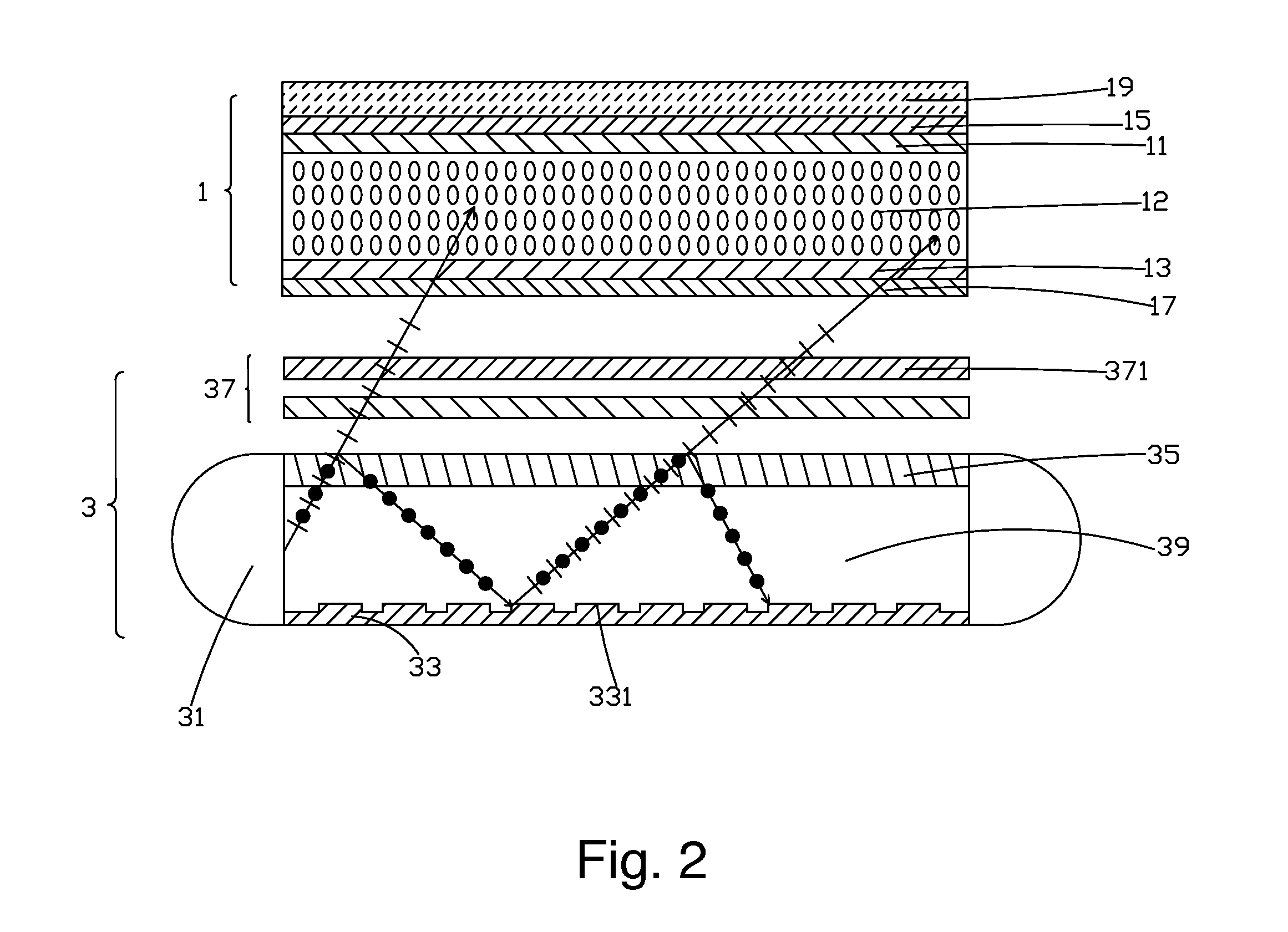
[0030]Referring to FIG. 2, a schematic view is given to illustrate the structure of a first embodiment of a liquid crystal display device according to the present invention. The liquid crystal display device comprises a liquid crystal panel 1 and a collimated exit light backlight module 3 that provides a light source to the liquid crystal panel 1.

[0031]The liquid crystal panel 1 comprises a color filter (CF) substrate 11, an array substrate 13 that is arranged opposite to the CF substrate 11, and a liquid crystal layer 12 that is filled between the CF substrate 11 and the array substrate 13. The CF substrate 11 has an upper surface that is distant away from the liquid crystal layer 12 in a relative sense and comprises an upper polarizer film 15 attached thereto and a l...


PUM


Abstract

The present invention provides a liquid crystal display device, which includes a liquid crystal panel (1) and a collimated exit light backlight module (3). The liquid crystal panel (1) includes a CF substrate (11), an array substrate (13), and a liquid crystal layer (12). The CF substrate (11) has an upper surface on which an upper polarizer film (15) is arranged. The array substrate (13) has a lower surface on which a lower polarizer film (17) is arranged. The upper polarizer film (15) includes a view angle diffusion film (19) arranged thereon. The collimated exit light backlight module (3) includes two backlight sources (31), a metallic grating reflector plate (33), a reflective polarizing beam splitter (35), and an optic film assembly (37). The two backlight sources (31), the metallic grating reflector plate (33), and the reflective polarizing beam splitter (35) collectively define a light guide chamber (39). The liquid crystal display device greatly improves light transmittance and light extraction efficiency and also effectively overcomes the issue of color deviation at a large view angle.

Description

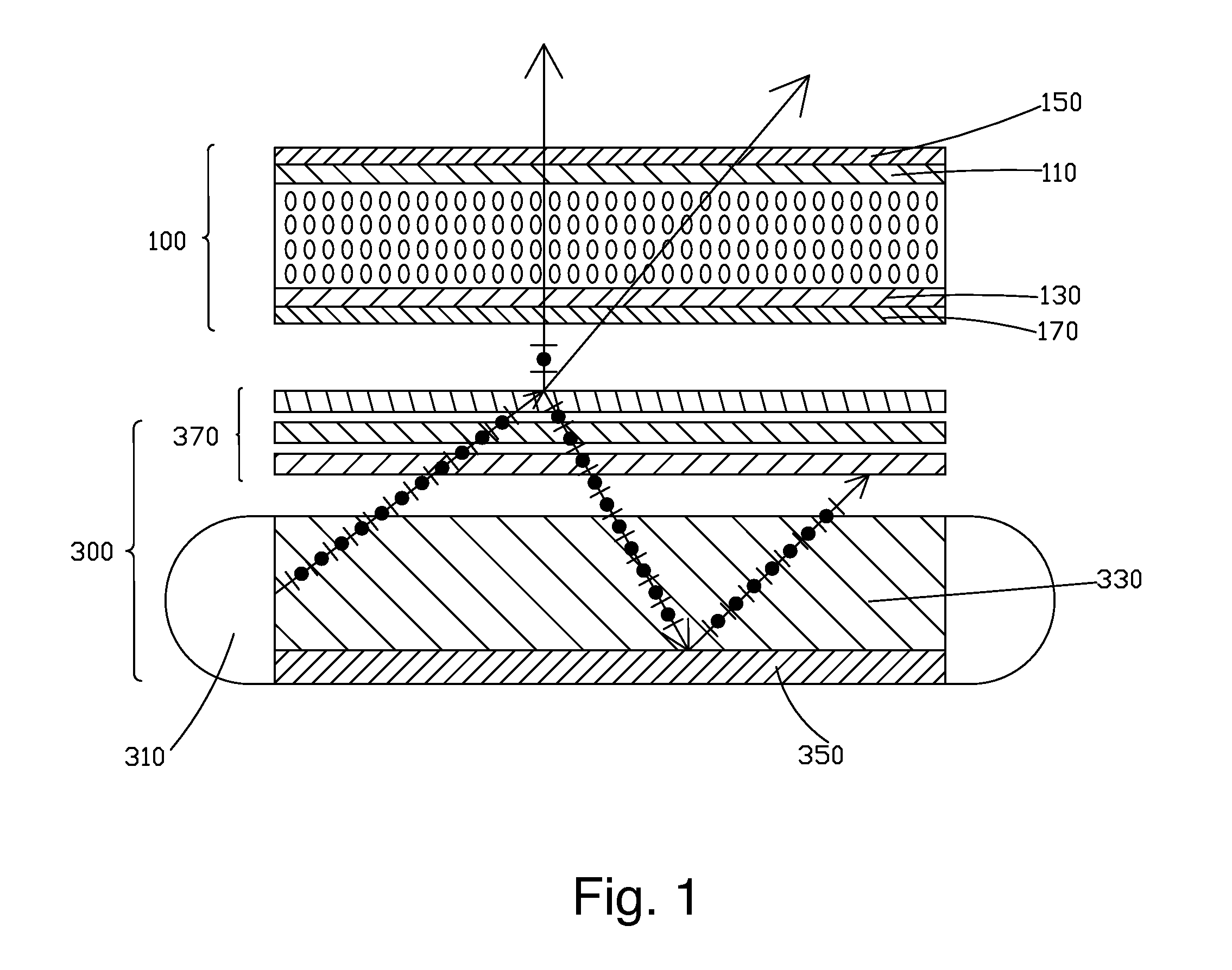
BACKGROUND OF THE INVENTION[0001]1. Field of the Invention[0002]The present invention relates to the field of liquid crystal display technology, and in particular to a liquid crystal display device.[0003]2. The Related Arts[0004]Liquid crystal displays (LCDs) have a variety of advantages, such as thin device body, low power consumption, and being free of radiation, and are thus of wide applications, such as liquid crystal televisions, mobile phones, personal digital assistants (PDAs), digital cameras, computer monitors, and notebook computer screens.[0005]Most of the currently available liquid crystal displays are backlighting liquid crystal displays, which comprise an enclosure, a liquid crystal panel arranged in the enclosure, and a backlight module mounted in the enclosure. The liquid crystal panel itself does not emit light and light must be supplied from the backlight module to the liquid crystal panel in order to normally display images[0006]FIG. 1 shows a schematic view of a ...

Claims


Application Information

Patent Timeline
IPC IPC(8): G02F1/1335F21V8/00
CPCG02F1/133504G02F1/133514G02F1/133536G02F1/133553G02F2001/133507G02B6/0056G02B6/0073G02B6/0053G02F2001/13355G02F1/133526G02B6/0055G02F1/133605G02F1/133615G02F1/133507
Inventor LIEN, SHUICHIHKANG, CHIHTSUNGKUO, YICHENG
Owner SHENZHEN CHINA STAR OPTOELECTRONICS TECH CO LTD
Learn More