Self-timed slc NAND pipeline and concurrent program without verification

a nand pipeline and program technology, applied in static storage, digital storage, instruments, etc., can solve the problems of mlc and tlc storage nand data reliability, performance, p/e endurance cycles of mlc and tlc, and slc storage is greatly degraded compared to slc storage, and achieves the effect of reducing the latencies of program and read

Active Publication Date: 2016-03-31
APLUS FLASH TECH
View PDF0 Cites 24 Cited by
  • Summary
  • Abstract
  • Description
  • Claims
  • Application Information

AI Technical Summary

Benefits of technology

[0011]The present invention is generally related to non-volatile NAND memory, regardless of 2D or 3D NANDs. Embodiments of the present invention provide a preferred multiple WLs SLC concurrent and pipeline program scheme without verification step based on a two(or more)-level hierarchical-BL NAND array structure. More specifically, a self-timed program-time Tpgm and discharge of Vpgm, Vpass, and Vread for each selected set of M WLs and top / bottom string-select translator gate control lines of each block-decoder for performing the program operation are also disclosed for providing more powerful and efficient mixed pipeline and concurrent program and read operations with both program and read latencies being reduced by more than M-fold.

Problems solved by technology

Unfortunately, when NAND manufacture technology scaling comes to below 30 nm, or even down to 1×nm-class range, interference coupling effect on the floating-gate charge threshold voltage Vt becomes very severe between two physically adjacent bit lines (BLs) and word lines (WLs) in aforementioned NAND arrays.
Thus the NAND data reliability, performance, and P / E endurance cycles of MLC and TLC are greatly degraded compared to SLC storage.
The Yupin coupling effect results in erroneous reading, which is not avoidable and much severe particularly in MLC and TLC NAND.
In some high-end industry or enterprise SSD code and data storage applications, the high bit errors and low P / E cycles cannot be accepted.
Firstly, the latency of whole cycle of the SLC program operation is about 30% increased when the SLC program verification is required.
Thirdly, the power consumption of the SLC iterative program and verification are increased proportional to the number of iteration steps, thus battery life is shortened in mobile system equipped with these SLC memory.

Method used


Image

  • Self-timed slc NAND pipeline and concurrent program without verification
  • Self-timed slc NAND pipeline and concurrent program without verification
  • Self-timed slc NAND pipeline and concurrent program without verification

Examples


Embodiment Construction

[0069]In the following detailed description of the present embodiments, reference is made to the accompanying drawings that forms a part hereof, and in which is shown, by way of illustration, specific embodiments in which the disclosure may be practiced. In the drawings, like numerals describe substantially similar components throughout the several views. These embodiments are described in sufficient detail to enable those skilled in the art to practice the embodiments. Other embodiments may be utilized and structural, logical, and electrical changes may be made without departing from the scope of the present disclosure. The following detailed description, therefore, not to be taken in a limitation sense.

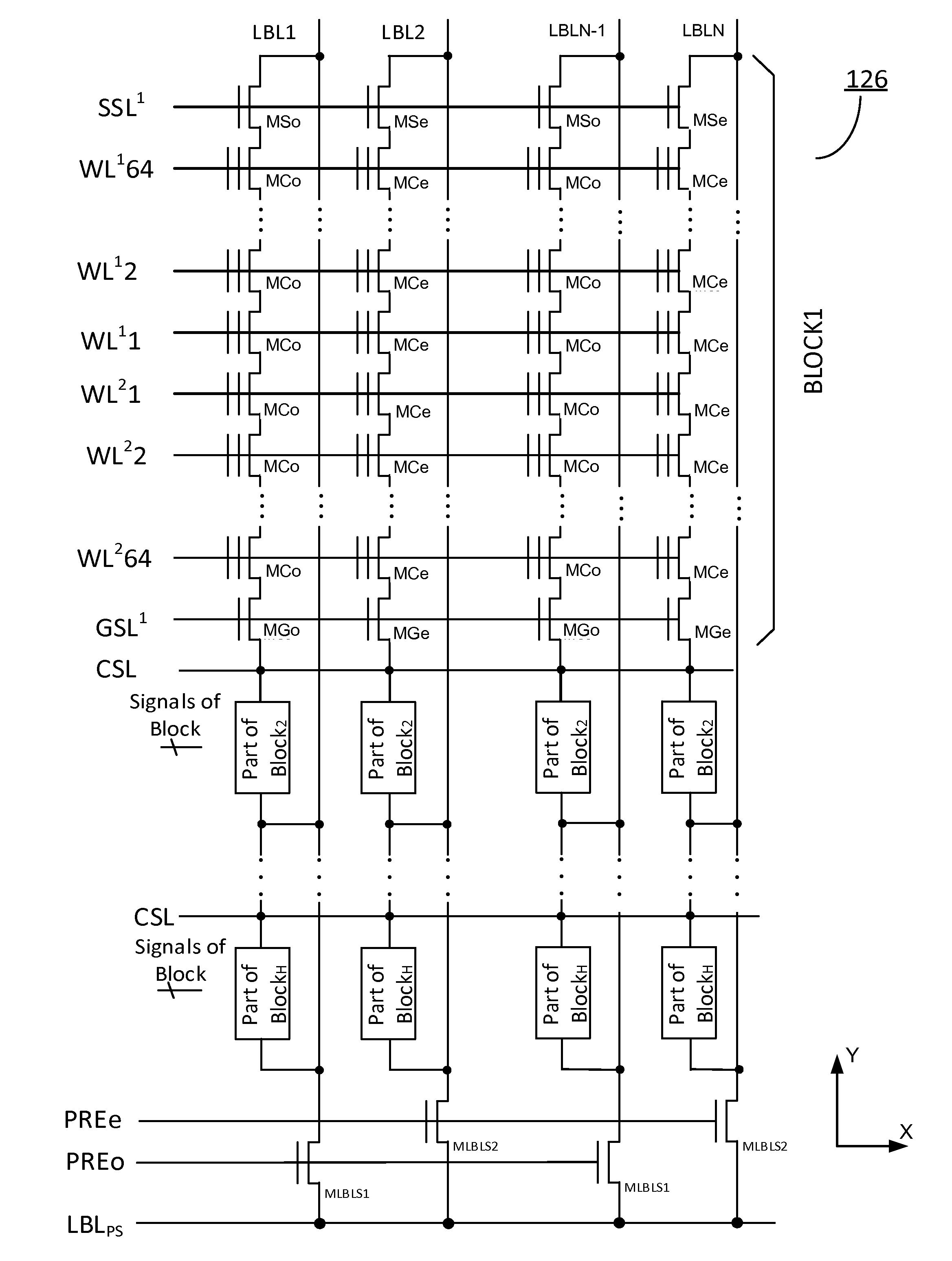
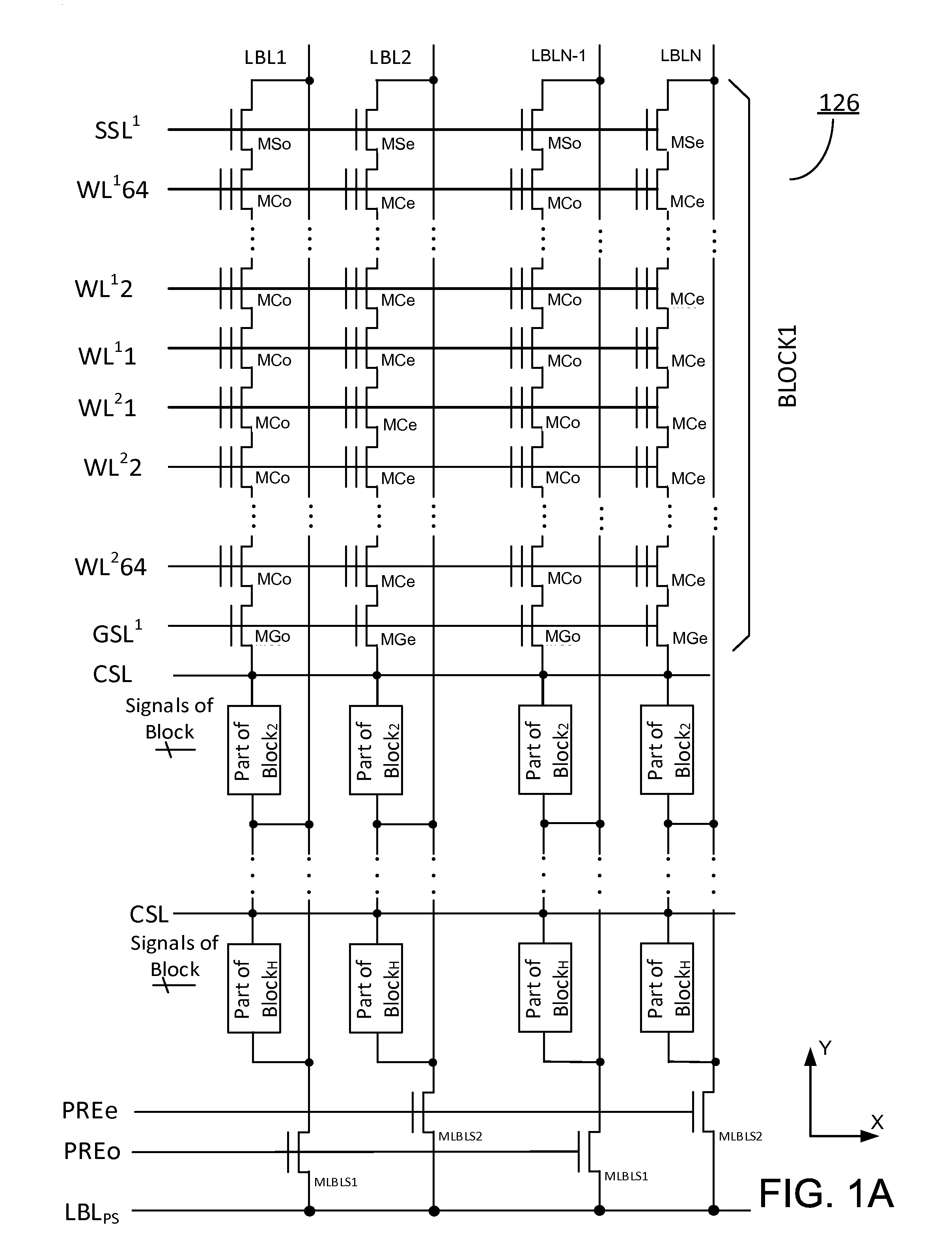
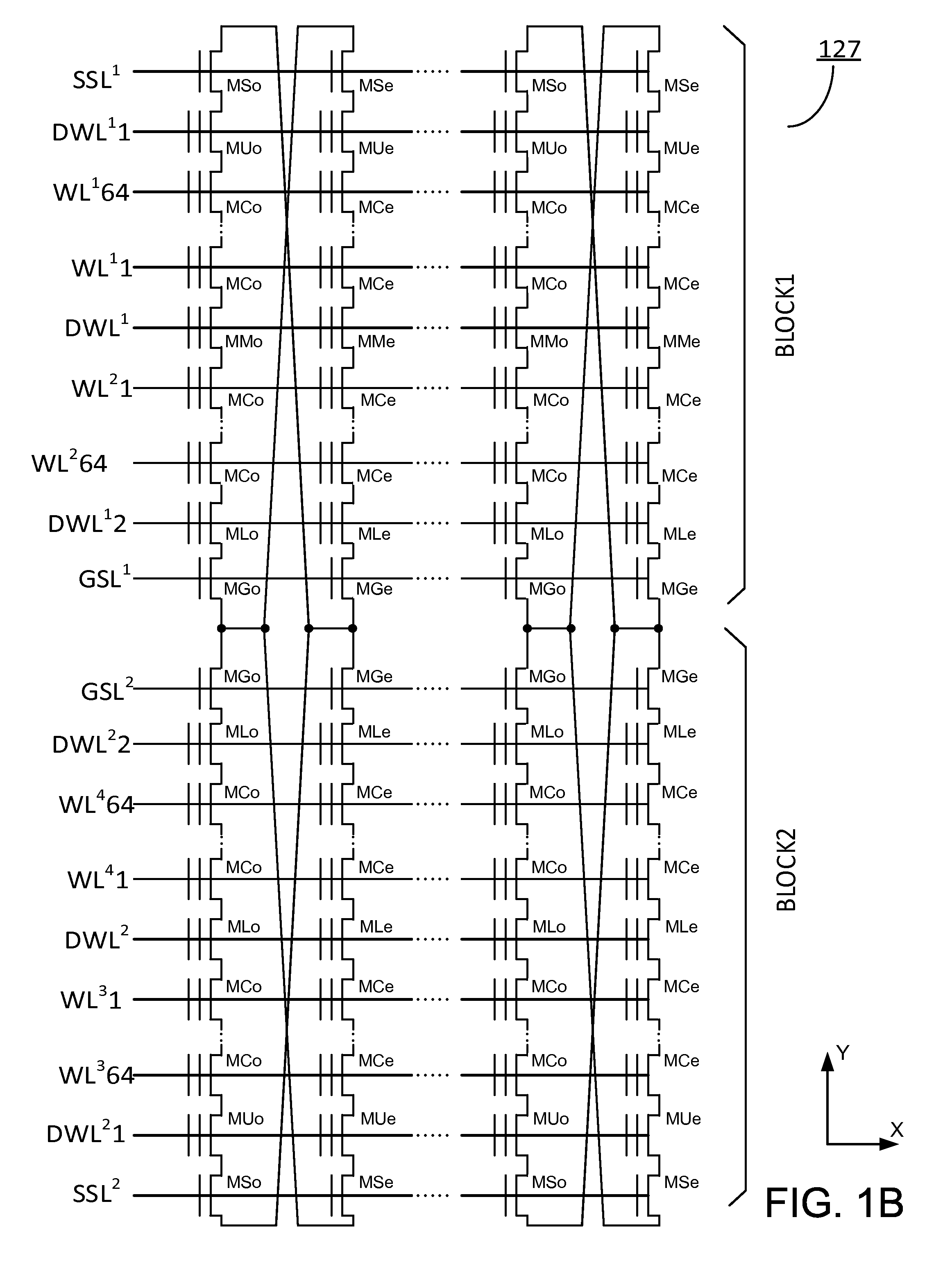
[0070]Through multiple embodiments, the present invention is to improve all aspects of non-pipeline and non-concurrent single SLC NAND program or single read operation in one plane of non-hierarchical legacy NAND, particularly for NAND design down to 20 nm, regardless of 2D or 3D NA...


PUM


Abstract

A hierarchical-GBL/LBL NAND array with a plurality of LG and MG groups in either orthogonal BL/CSL scheme or parallel BL/SL scheme including a plurality of block-decoders with a shared self-timed delay control circuit and a plurality of fully-shielding dynamic CACHE registers made of 2 local broken metal lines within the array and DRAM-like SA is provided. Each DCR capacitor is flexibly expandable by connecting multiple CLGs made by the local broken metal lines of the LGs to form a CMG of a larger MG. Based on the NAND array, multiple randomly selected WLs in multiple random blocks within multiple random LGs within one MG can be selected on basis of one WL per block per LG for performing an ABL pipeline and concurrent SLC program without verification, and on basis of one WL per block per MG for performing an ABL-like or HBL pipeline and concurrent SLC read.

Description

1. CROSS-REFERENCES TO RELATED APPLICATIONS[0001]This application claims priority to U.S. Provisional Application No. 62 / 056,590, filed Sep. 18, 2014, commonly assigned and incorporated by reference herein for all purposes.[0002]This application is related to U.S. patent application Ser. Nos. 14 / 806,629, 14 / 583,178, 14 / 487,078, 14 / 341,739, 14 / 316,936, 14 / 283,209, and 14 / 828,427, incorporated by reference herein for all purposes.2. BACKGROUND OF THE INVENTION[0003]Electrically Erasable and Programmable NAND memory has become one of the most popular non-volatile memory (NVM) with the lowest unit price and highest density. Particularly, NAND is extensively used with a big volume in cellular phones, digital cameras, personal digital assistants, mobile computing devices, tablet, SSD, and desktop computers, and many other emerging wearable devices. In order to keep driving NAND density higher at a lower unit cost, the program schemes of MLC, TLC, and even XLC are extensively used in 2D NA...

Claims


Application Information

Patent Timeline
Patent Type & Authority Applications(United States)
IPC IPC(8): G11C16/10G11C16/04G11C16/08G11C16/26G11C16/32G11C16/34
CPCG11C16/10G11C16/0483G11C16/08G11C16/32G11C16/3459G11C16/0466G11C16/0408G11C16/26G11C16/24
Inventor LEE, PETER, WUNG
Owner APLUS FLASH TECH
Why Eureka
Try Eureka