Semiconductor device and display device

a technology of semiconductor devices and display devices, applied in semiconductor devices, electrical devices, instruments, etc., can solve the problems of reducing the display quality of a display device, and the difficulty of driving transistors of a large number of different pixels, and achieve the effect of small power consumption and high accuracy

Active Publication Date: 2016-03-31
SEMICON ENERGY LAB CO LTD
View PDF15 Cites 21 Cited by
  • Summary
  • Abstract
  • Description
  • Claims
  • Application Information

AI Technical Summary

Benefits of technology

[0027]According to one embodiment of the present invention, a semiconductor device capable of detecting a minute current with high accuracy can be provided. According to one embodiment of the present invention, a semiconductor device capable of detecting a minute current with small power consumption can be provided. According to one embodiment of the present invention, a novel semiconductor device or an operation method of a novel semiconductor device can be provided.
[0028]Note that the description of the plurality of effects does not preclude the existence of other effects. In one embodiment of the present invention, there is no need to achieve all the effects described above. In one embodiment of the present invention, an object other than the above objects, an effect other than the above effects, and a novel feature will be apparent from the description of the specification and the drawings.

Problems solved by technology

Variations in electrical characteristics of the driving transistor among a plurality of pixels are one of the causes of reduction in display quality of a display device.
It is very difficult for driving transistors of a large number of different pixels to have perfectly the same electrical characteristics.

Method used


Image

  • Semiconductor device and display device
  • Semiconductor device and display device
  • Semiconductor device and display device

Examples


embodiment 1

[0050]In this embodiment, a semiconductor device of one embodiment of the present invention will be described with reference to FIGS. 1 to 6.

>

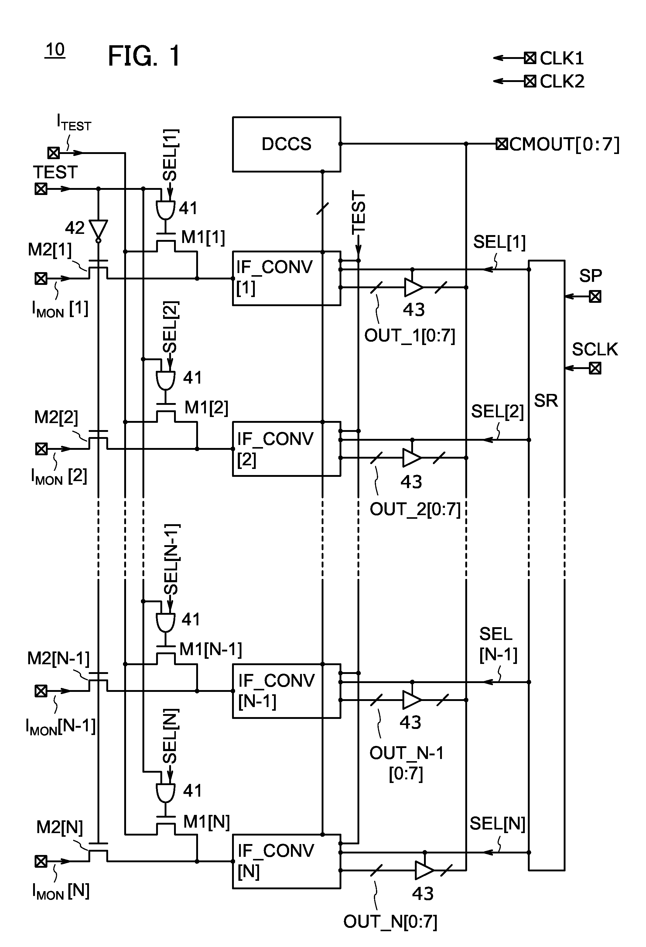
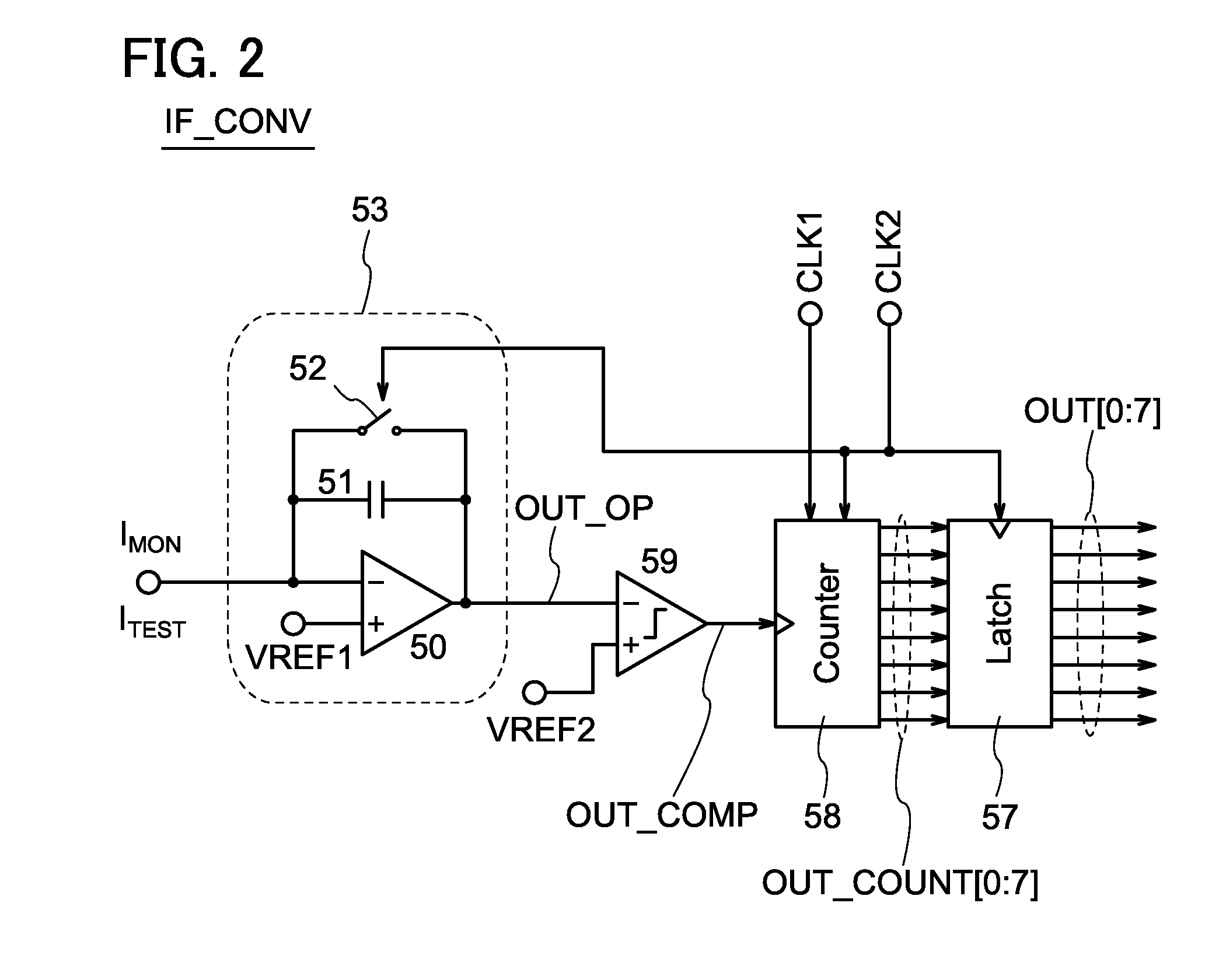
[0051]FIG. 1 is a circuit diagram showing a configuration example of a semiconductor device 10. The semiconductor device 10 includes a plurality of transistors M1 (M1[1] to M1[N], where N is a natural number of 1 or more), a plurality of transistors M2 (M2[1] to M2[N], an inverter 42, a plurality of ANDs 41, a plurality of circuits IF_CONV (IF_CONV[1] to IF_CONV[N]), a circuit DCCS (digital calibration control system), a plurality of TRIBUFs (tri-state buffer circuits) 43, and a circuit SR (shift register).

[0052]Although the description below will be made regarding the transistors M1 and the transistors M2 as n-channel transistors, one embodiment of the present invention can be used in the case where the transistors M1 and the transistors M2 are p-channel transistors.

[0053]Signals IMON (IMON[1] to IMON[N]) in FIG. 1 each include the value of a...

embodiment 2

[0144]In this embodiment, an example of a display device that includes the semiconductor device 10 or the semiconductor device 20 described in Embodiment 1 will be described.

>

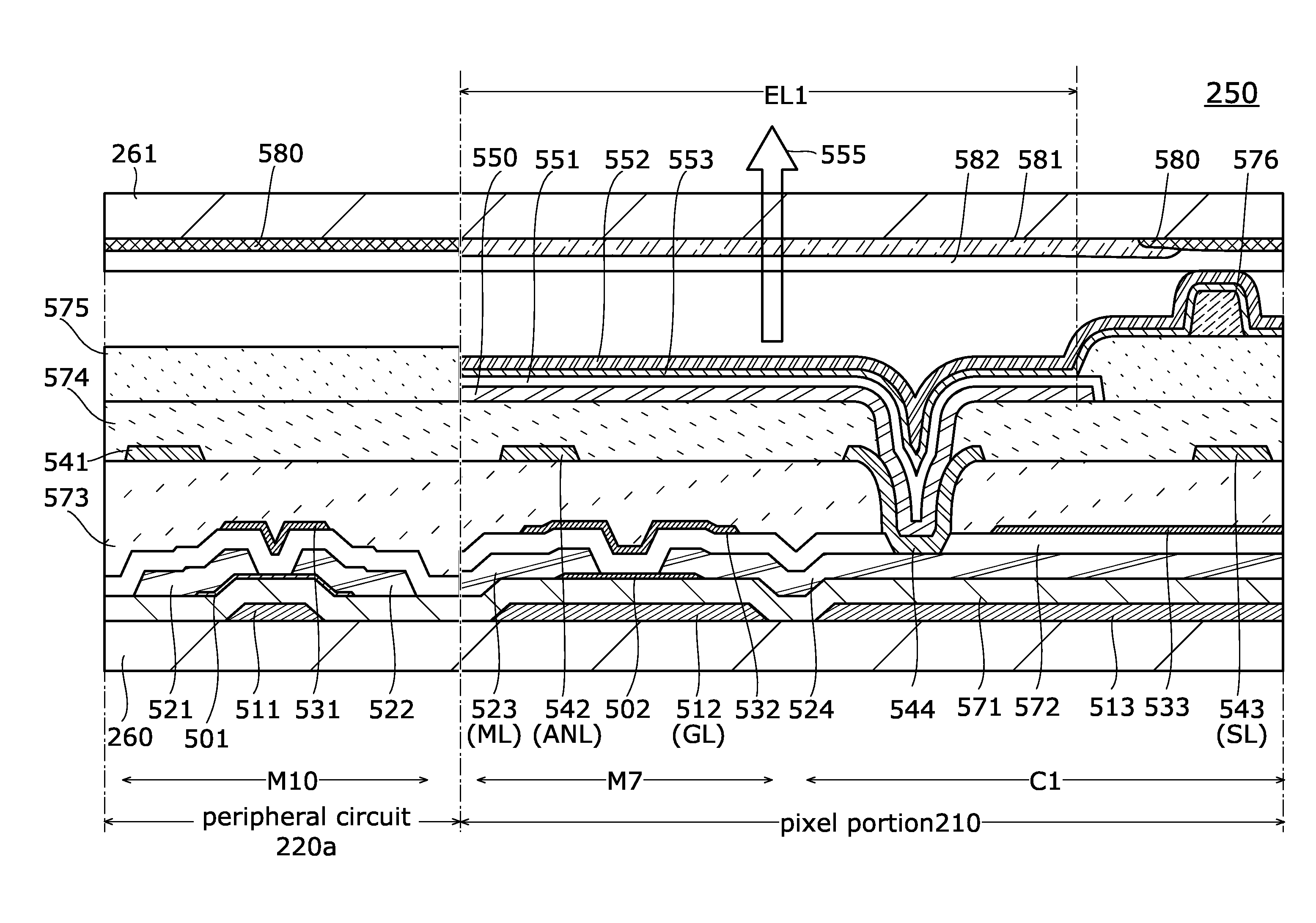
[0145]FIG. 7 is a block diagram illustrating a configuration example of a display device. The display device 200 includes a pixel portion 210, a peripheral circuit 220, a CPU 230, a control circuit 231, a power supply circuit 232, an image processing circuit 233, and a memory 234.

[0146]The CPU 230 is a circuit for executing an instruction and controlling the display device 200 collectively. The CPU 230 executes an instruction input from the outside and an instruction stored in an internal memory. The CPU 230 generates signals for controlling the control circuit 231 and the image processing circuit 233. On the basis of a control signal from the CPU 230, the control circuit 231 controls the operation of the display device 200. The control circuit 231 controls the peripheral circuit 220, the power supply circuit 2...

operation example

[0167]The data signal Vda is input to the wiring SL. The voltage value of the data signal Vda corresponds to the gray scale of the video signal. In FIG. 10B, Vda[k] and Vda[k+1] represent the data signals Vda input to the k-th pixel 211 and the (k+1)-th pixel 211, respectively.

[0168]A period P1 is a writing operation period and the light-emitting element EL1 does not emit light during the period. Voltage Vano is applied to the wiring ANL and voltage Vcat is applied to the cathode of the light-emitting element EL1. The wiring ML is electrically connected to a power supply line supplying voltage V0. The wiring GL is set at a high level to turn on the transistors M5 and M6. Voltage Vda of the wiring SL is supplied to the node N2. A drain current of which the amount corresponds to that of the voltage Vda flows in the transistor M6.

[0169]Note that the voltage Vano, the voltage V0, and the voltage Vcat are preferably set so as to satisfy the following formulae (b1), (b2), and (b3). In the...


PUM


Abstract

A semiconductor device capable of detecting a minute current with high accuracy is provided. The semiconductor device includes a first circuit, a second circuit, a first transistor, and a second transistor. A first analog signal is input to the first circuit via the first transistor. A second analog signal is input to the first circuit via the second transistor. The first analog signal includes a value of a first current. The second analog signal includes a value of a second current. The first circuit is capable of converting the first analog signal into a first digital signal. The second circuit is capable of generating a second digital signal based on the first digital signal. The first circuit is capable of converting the second analog signal into a third digital signal based on the second digital signal. The first or second transistor includes an oxide semiconductor in a channel.

Description

BACKGROUND OF THE INVENTION[0001]1. Field of the Invention[0002]One embodiment of the present invention relates to a semiconductor device, a display device, or an electronic device. Further, one embodiment of the present invention relates to, for example, a circuit, a processing circuit, or a memory circuit, which utilizes a semiconductor, a driving method thereof, a manufacturing method thereof, or the like.[0003]2. Description of the Related Art[0004]For pixels of an active matrix display device using light-emitting elements, a variety of circuit configurations have been proposed. In general, at least a light-emitting element, a transistor that controls input of a video signal to a pixel, and a transistor (driving transistor) that controls current supplied to the light-emitting element are provided in the pixel. Supplying a drain current flowing through the driving transistor to the light-emitting element enables the light-emitting element to emit light with a luminance correspond...

Claims


Application Information

Patent Timeline
Patent Type & Authority Applications(United States)
IPC IPC(8): H01L27/12
CPCH01L27/1225G09G3/3233G09G2320/0295G09G2320/043
Inventor TAKAHASHI, KEI
Owner SEMICON ENERGY LAB CO LTD
Why Eureka
Try Eureka