Thin film transistor substrate and display apparatus using the same

a technology of thin film transistors and substrates, applied in thermoelectric devices, non-linear optics, instruments, etc., can solve problems such as complex processes, and achieve the effect of reducing the number of mask processes

Active Publication Date: 2016-03-31
LG DISPLAY CO LTD
View PDF7 Cites 46 Cited by
  • Summary
  • Abstract
  • Description
  • Claims
  • Application Information

AI Technical Summary

Benefits of technology

[0034]An aspect of the present invention is directed to provide a TFT substrate, a method of manufacturing the same, and a display apparatus using the same, in which the number of mask processes is reduced.

Problems solved by technology

As described above, in the related art TFT substrate, since a total eleven-time mask process is needed, a process is very complicated.

Method used


Image

  • Thin film transistor substrate and display apparatus using the same
  • Thin film transistor substrate and display apparatus using the same
  • Thin film transistor substrate and display apparatus using the same

Examples


Embodiment Construction

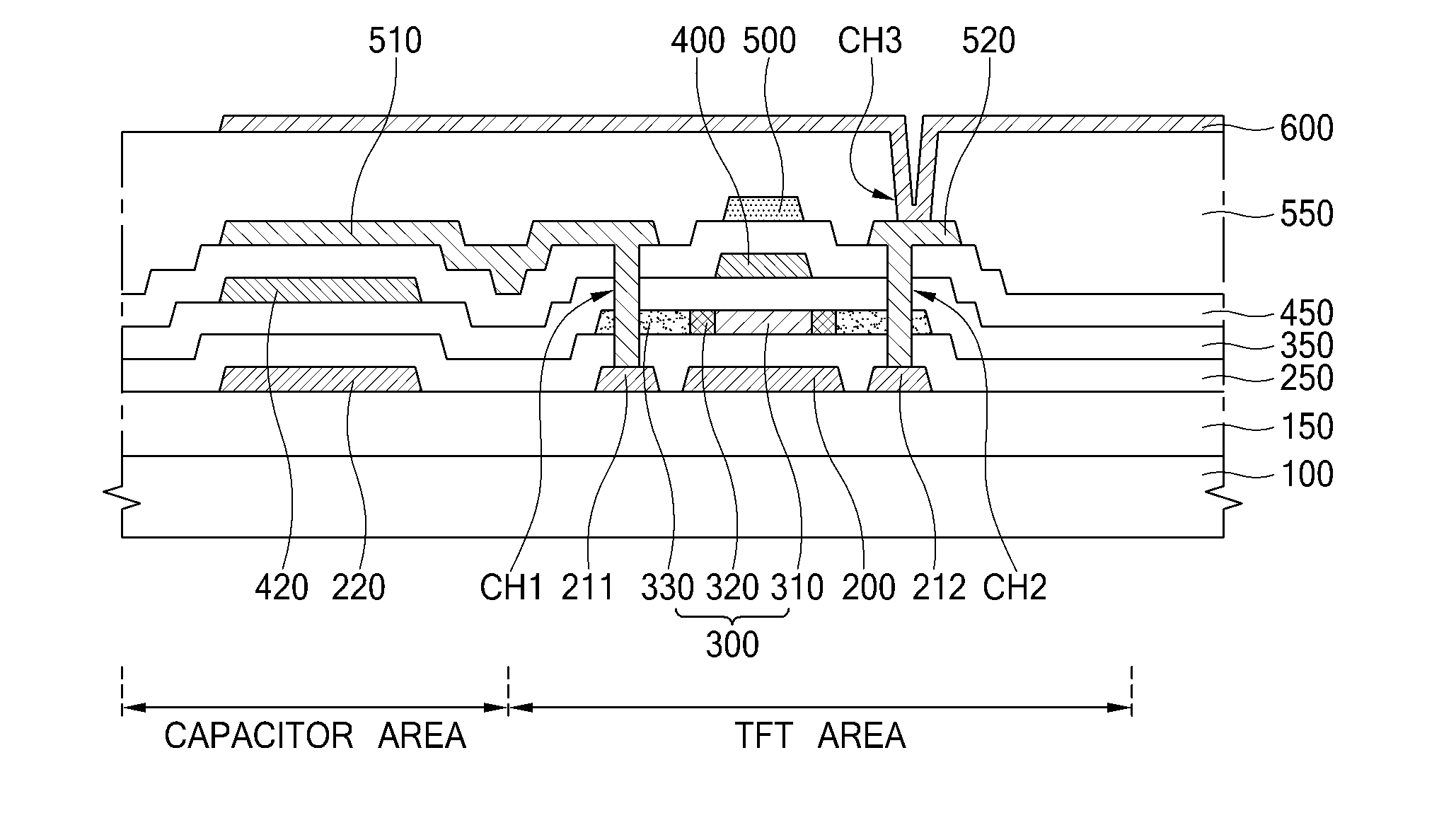
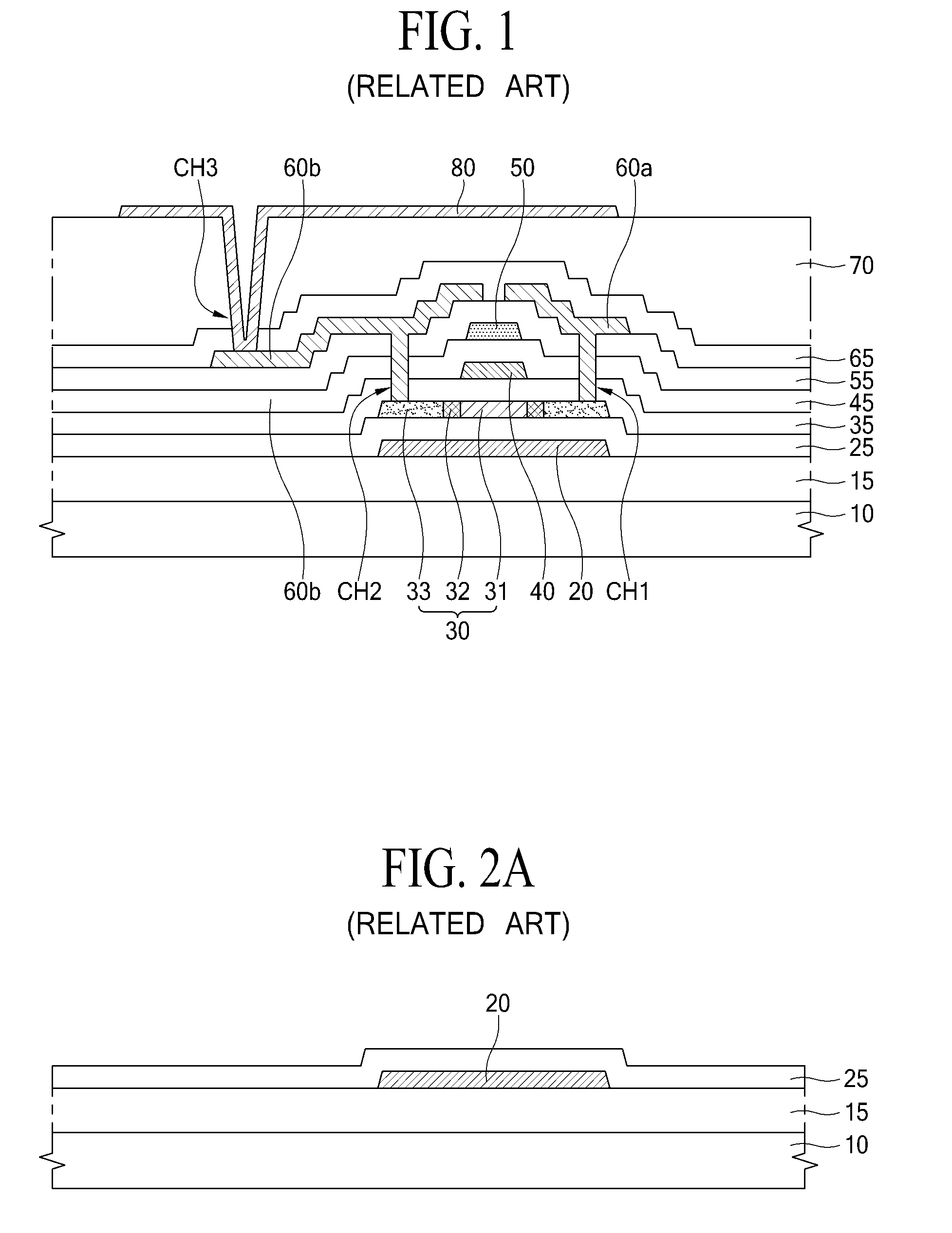
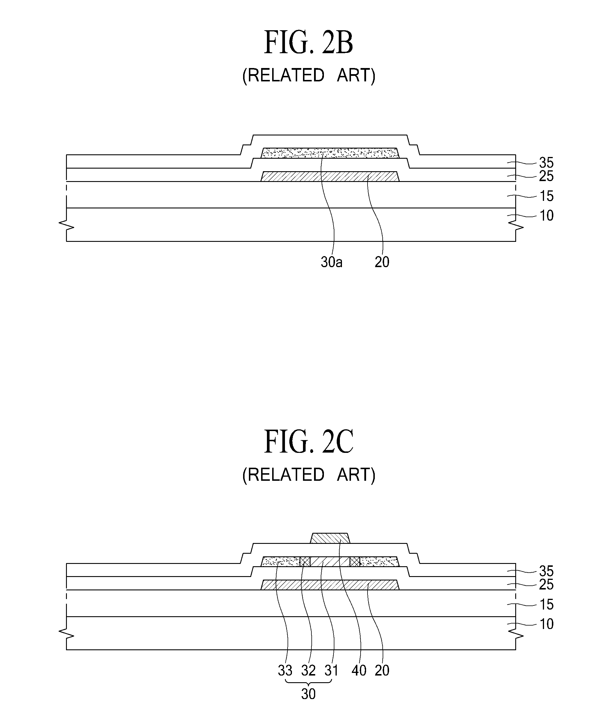
[0063]Reference will now be made in detail to the exemplary embodiments of the present invention, examples of which are illustrated in the accompanying drawings. Wherever possible, the same reference numbers will be used throughout the drawings to refer to the same or like parts.

[0064]Advantages and features of the present invention, and implementation methods thereof will be clarified through following embodiments described with reference to the accompanying drawings. The present invention may, however, be embodied in different forms and should not be construed as limited to the embodiments set forth herein. Rather, these embodiments are provided so that this disclosure will be thorough and complete, and will fully convey the scope of the present invention to those skilled in the art. Further, the present invention is only defined by scopes of claims.

[0065]A shape, a size, a ratio, an angle, and a number disclosed in the drawings for describing embodiments of the present invention ...


PUM

PropertyMeasurementUnit
doping concentrationaaaaaaaaaa
concentrationaaaaaaaaaa
structureaaaaaaaaaa

Abstract

A thin film transistor (TFT) substrate is disclosed. The TFT substrate includes a substrate, a blocking layer, a source electrode, and a drain electrode on a same layer over the substrate, an active layer overlapping the blocking layer, the source electrode, and the drain electrode, a gate insulation layer over the active layer, a first gate electrode over the gate insulation layer, an interlayer dielectric over the first gate electrode, a first connection electrode over the interlayer dielectric and connected to the active layer and the source electrode through a first contact hole, a second connection electrode over the interlayer dielectric and connected to the active layer and the drain electrode through a second contact hole, a planarization layer over the first connection electrode and the second connection electrode, and a pixel electrode over the planarization layer and connected to the second connection electrode through a third contact hole.

Description

CROSS-REFERENCE TO RELATED APPLICATIONS[0001]This application claims the benefit of the Korean Patent Application No. 10-2014-0131762 filed on Sep. 30, 2014, which is hereby incorporated by reference for all purposes as if fully set forth herein.BACKGROUND OF THE INVENTION[0002]1. Field of the Invention[0003]The present invention relates to a thin film transistor (TFT) substrate. More particularly, the present invention relates to a TFT substrate applied to a flexible display apparatus.[0004]2. Discussion of the Related Art[0005]Thin film transistors (TFTs) are being widely used as switching devices of display apparatuses such as liquid crystal display (LCD) apparatuses, organic light emitting display apparatuses, etc. Therefore, a TFT substrate where a plurality of TFTs are formed is a fundamental element of a display apparatus.[0006]Research on flexible display apparatuses is being actively done. Since it is required for the flexible display apparatuses to be bent or wound, instea...

Claims


Application Information

Patent Timeline
Patent Type & Authority Applications(United States)
IPC IPC(8): H01L27/12G02F1/1362G02F1/1368H01L27/32H01L29/786
CPCG02F1/136286G02F1/136227G02F1/136209G02F1/1368H01L29/78612H01L29/78696H01L27/3248H01L27/1255H01L29/41733H01L29/66757H01L29/78621H01L29/78633H01L29/78645G02F1/136213G02F1/133357H10K59/126H01L29/66742H01L29/78603H10K59/123
Inventor KIM, HYUN, HOKIM, WOO, JOON
Owner LG DISPLAY CO LTD
Why Eureka
Try Eureka