Semiconductor structures and fabrication method thereof

a technology of semiconductor devices and semiconductor structures, applied in the direction of semiconductor devices, electrical equipment, transistors, etc., can solve the problems of leakage current, poor structural appearance of transistors, and affecting the electrical properties of semiconductor devices

Active Publication Date: 2016-03-31
SEMICON MFG INT (SHANGHAI) CORP
View PDF1 Cites 3 Cited by
  • Summary
  • Abstract
  • Description
  • Claims
  • Application Information

AI Technical Summary

Problems solved by technology

However, a shorter gate in a transistor may cause short channel effect, thus leads to a leakage current in the transistor and eventually affects the electrical properties of the semiconductor device.
However, for transistors fabricated by using the existing method with a stress layer formed in the source region and the drain region, the structural appearance of the transistor may be poor and the performance may be unstable.
Specifically, following an existing method, EPI particles, also known as mushroom defects, are often formed on the surface of the semiconductor device close to the gate, which may cause a leakage current on the top of the gate layer or the subsequently-formed metal gate.
Thus, the performance of the transistor may be unstable, the reliability may be low, and the yield may also decrease.

Method used


Image

  • Semiconductor structures and fabrication method thereof
  • Semiconductor structures and fabrication method thereof
  • Semiconductor structures and fabrication method thereof

Examples


Embodiment Construction

[0013]Reference will now be made in detail to exemplary embodiments of the invention, which are illustrated in the accompanying drawings. Wherever possible, the same reference numbers will be used throughout the drawings to refer to the same or like parts.

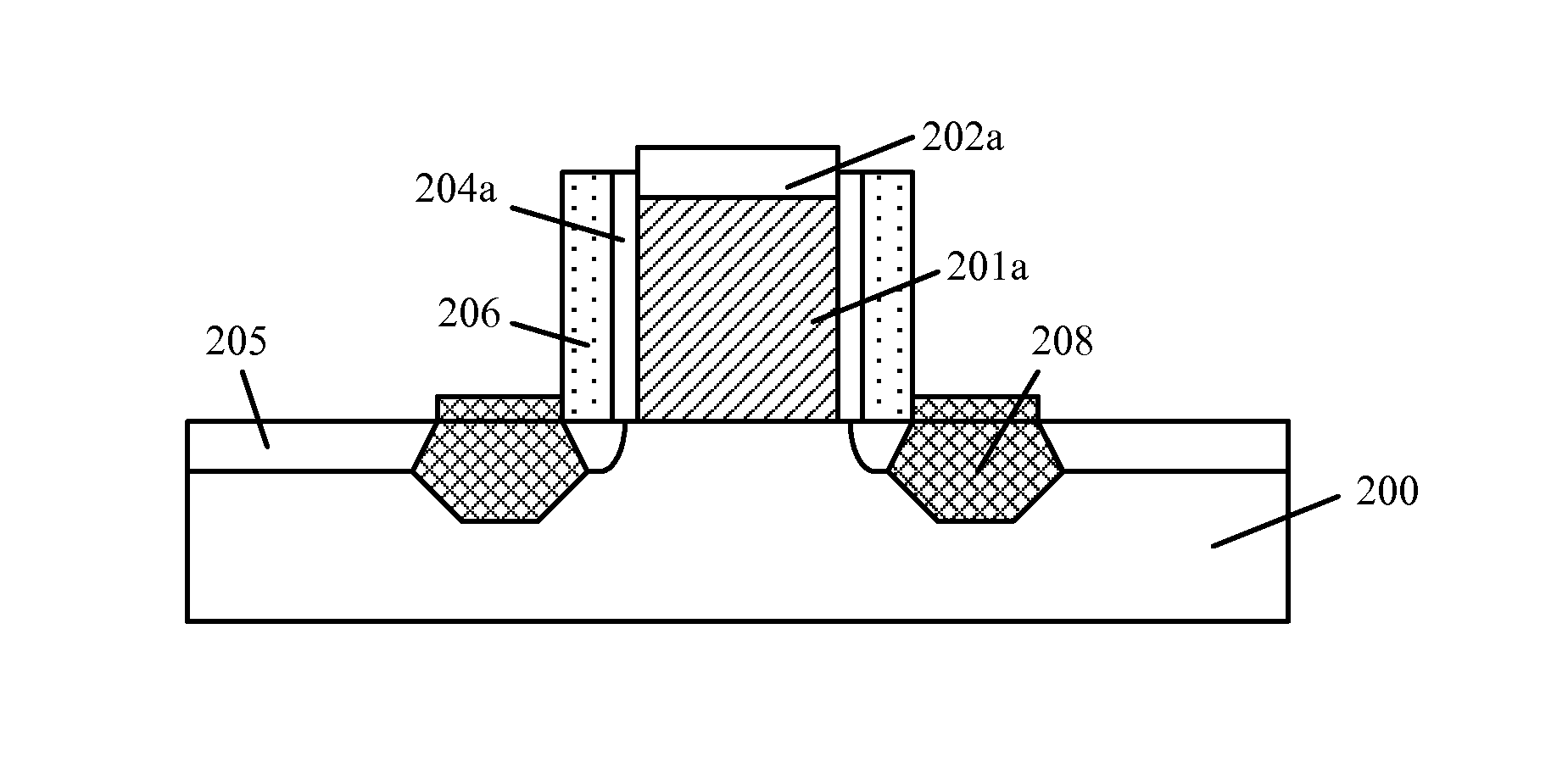
[0014]In current technology, a stress layer may be formed in both the source region and the drain region of a transistor to improve the mobility of carriers in the channel region thus avoid the short channel effect as the dimensions of the transistor become shorter than in the past.

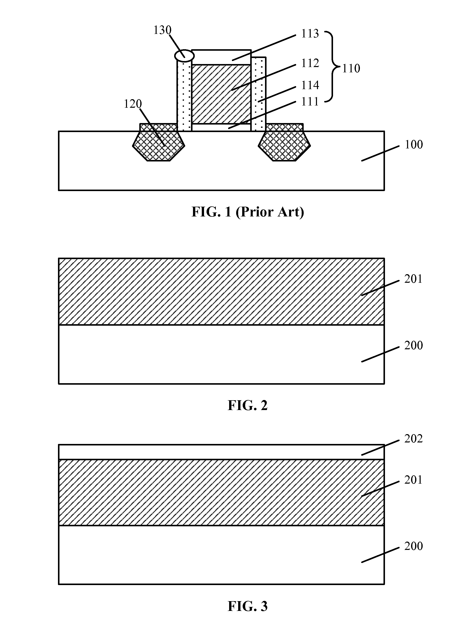
[0015]FIG. 1 illustrates a cross-section view of a transistor of an existing method. As shown in FIG. 1, the structure of the transistor includes a substrate 100 with a gate structure 110 on a top surface of the substrate 100. The gate structure 110 consists of a gate dielectric layer 111 formed on the top surface of the substrate 100, a gate layer 112 formed on the surface of the gate dielectric layer 111, a mask layer 113 formed on the top of the gate ...


PUM


Abstract

A method is provided for fabricating transistors. The method includes providing a semiconductor substrate. The substrate has a gate film and a mask film formed on a top surface. The mask film contains implanted carbon ions. The method further includes forming a mask layer by etching the mask film and then forming a gate layer by etching through the gate film using the mask layer as a mask until the substrate is exposed. The method also includes forming a first sidewall containing implanted carbon ions on the side surface of the gate layer and the mask layer; forming a stress layer in the substrate on both sides of the gate layer and the first side-wall; and forming a source region on one side of the gate layer and the first sidewall and a drain region on the other side of the gate layer and the first side wall.

Description

CROSS-REFERENCES TO RELATED APPLICATIONS[0001]This application claims the priority of Chinese patent application No. 201410504707.6, filed on Sep. 26, 2014, the entirety of which is incorporated herein by reference.FIELD OF THE INVENTION[0002]The present invention generally relates to the field of semiconductor manufacturing technology and, more particularly, relates to semiconductor transistors and fabrication processes thereof.BACKGROUND[0003]With the rapid development of semiconductor manufacturing technology, semiconductor devices are now moving towards the direction of higher element density and higher integration degree. As the most fundamental semiconductor device, transistor is currently being widely used. Along with the improvement-of the element density and the integrity of semiconductor devices, the dimensions of the gate in transistors thus become much shorter than in the past. However, a shorter gate in a transistor may cause short channel effect, thus leads to a leakag...

Claims


Application Information

Patent Timeline
Patent Type & Authority Applications(United States)
IPC IPC(8): H01L29/66H01L29/78
CPCH01L29/66636H01L29/7848H01L29/66492H01L21/265H01L29/165H01L29/4983H01L29/6656H01L29/6659H01L29/7834
Inventor HAN, QIUHUACHEN, JIE
Owner SEMICON MFG INT (SHANGHAI) CORP
Why Eureka
Try Eureka