Optical module, optical transceiver, printed circuit board, and flexible printed circuit board

a technology of optical transceivers and printed circuit boards, applied in the direction of printed circuit non-printed electric components, high frequency circuit adaptations, instruments, etc., can solve problems such as signal degradation, and achieve the effect of reducing reflection and radiation and reducing the degradation of electrical signals

Active Publication Date: 2016-03-31
LUMENTUM JAPAN INC
View PDF2 Cites 15 Cited by
  • Summary
  • Abstract
  • Description
  • Claims
  • Application Information

AI Technical Summary

Benefits of technology

[0026]According to the one embodiment of the present invention, the optical module, the optical transceiver module, the printed circuit board, and the flexible printed circuit board for reducing the reflection and radiation at the connection position, to thereby reduce the signal degradation of the electrical signal to be transmitted, are provided.

Problems solved by technology

In general, a high frequency electrical signal is reflected or radiated at a connection position between transmission lines, and signal degradation occurs in the electrical signal propagating in an optical module.

Method used


Image

  • Optical module, optical transceiver, printed circuit board, and flexible printed circuit board
  • Optical module, optical transceiver, printed circuit board, and flexible printed circuit board
  • Optical module, optical transceiver, printed circuit board, and flexible printed circuit board

Examples


first embodiment

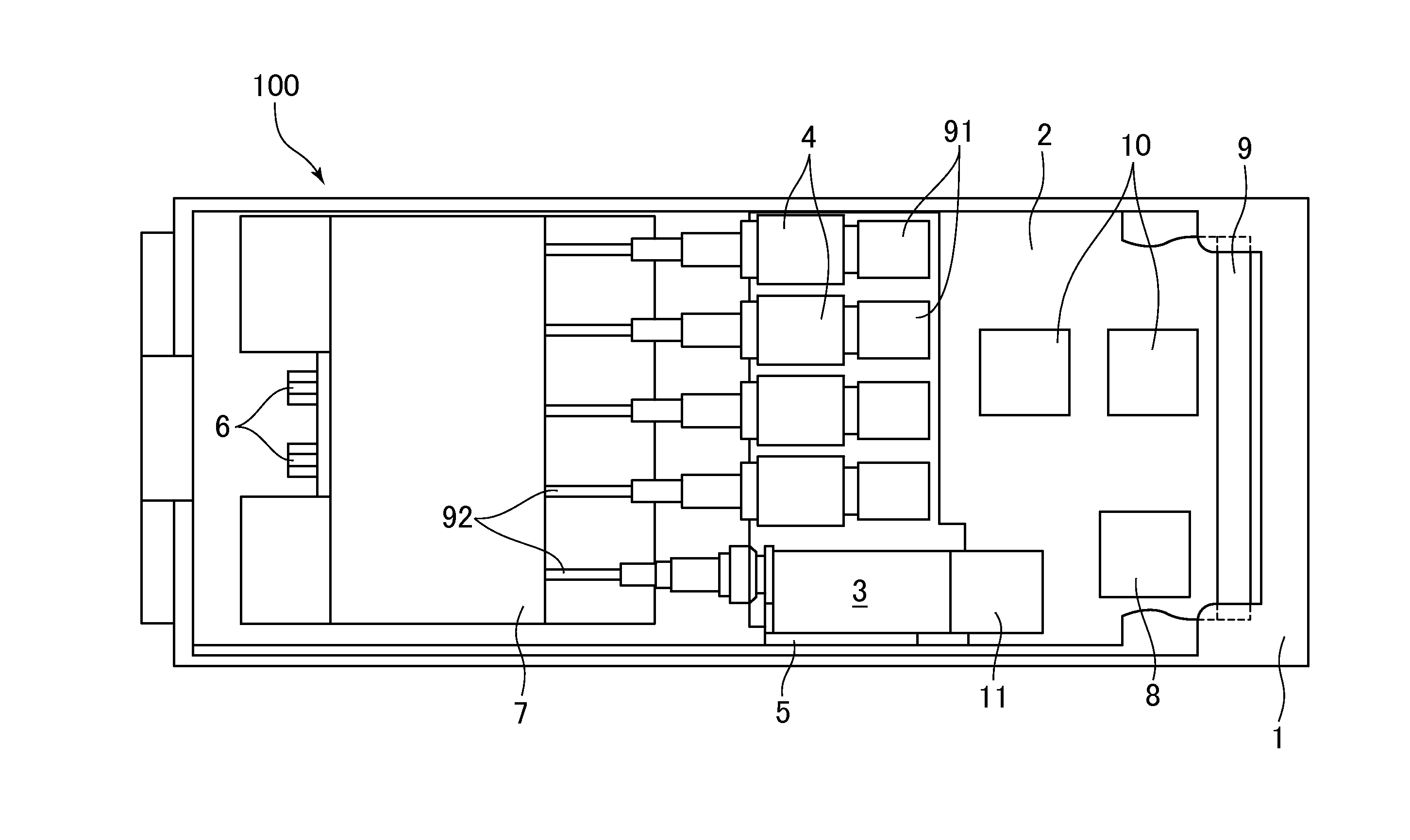
[0056]FIG. 1 is a plan view of an optical transceiver module 100 according to a first embodiment of the present invention. FIG. 1 is a view for schematically illustrating components stored inside a housing of the optical transceiver module 100. Specifically, FIG. 1 is an illustration of a state in which a top plate (plate member on a side on which an optical reception component 3, optical transmission components 4, and the like are mounted with respect to a printed circuit 2) of a housing 1 is removed. Note that, the optical transceiver module 100 according to this embodiment has exterior dimensions compliant with the CFP2 standard, but may be an optical module compliant with another standard or an optical transceiver module having an original size that is not compliant with any standard.

[0057]As illustrated in FIG. 1, a printed circuit board (PCB) 2 having a flat plate shape is fixed inside the housing 1, and the optical reception component (ROSA) 3 and the optical transmission com...

second embodiment

[0082]FIG. 8A and FIG. 8B are respectively a plan view and a bottom view of an end part of a printed circuit board 2 (first circuit board) according to a second embodiment of the present invention. FIG. 9A and FIG. 9B are respectively a plan view and a bottom view of an end part of a flexible printed circuit board 11 (second circuit board) according to this embodiment. In the first embodiment, the single-ended transmission line is formed on the circuit board, but in this embodiment, a differential transmission line is formed on the circuit board. As a result, the configurations of the printed circuit board 2 and the flexible printed circuit board 11 according to this embodiment are different from those of the first embodiment in the following points, but the other configurations are the same as those of the first embodiment.

[0083]As illustrated in FIG. 8A, the first signal terminal part includes a pair of (two) first signal terminals 21A and 21B extending in the longitudinal directi...

third embodiment

[0086]FIG. 10A and FIG. 10B are respectively a plan view and a bottom view of an end part of a printed circuit board 2 (first circuit board) according to a third embodiment of the present invention. FIG. 11A and FIG. 11B are respectively a plan view and a bottom view of an end part of a flexible printed circuit board 11 (second circuit board) according to this embodiment. In the first embodiment, the first ground terminal part, the first through ground conductors, the second ground terminal part, and the second through ground conductors are formed only in the fourth region in the third region, but in this embodiment, the first ground terminal part, the first through ground conductors, the second ground terminal part, and the second through ground conductors are each formed further in the fifth region. As a result, the configurations of the printed circuit board 2 and the flexible printed circuit board 11 according to this embodiment are different from those of the first embodiment i...


PUM


Abstract

An optical module includes: a first circuit board including a first signal terminal part and a first ground terminal part formed on a front surface; and a second circuit board including a second signal terminal part and a second ground terminal part formed on a back surface. The first circuit board further includes: a first dielectric layer; a first signal wire formed on a front surface of the first dielectric layer; a first ground conductor layer formed on a back surface of the first dielectric layer; and a first through ground conductor passing through the first dielectric layer. The first ground terminal part is formed, in a first region and a second region respectively located on both sides of the first signal terminal part in a first direction, and in a third region prescribed at a location beyond the first signal terminal part in a second direction.

Description

CROSS-REFERENCE TO RELATED APPLICATION[0001]The present application claims priority from Japanese application JP 2014-202188 filed on Sep. 30, 2014, the content of which is hereby incorporated by reference into this application.BACKGROUND OF THE INVENTION[0002]1. Field of the Invention[0003]The present invention relates to an optical module, an optical transceiver, a printed circuit board, and a flexible printed circuit board.[0004]2. Description of the Related Art[0005]An optical module includes optical high frequency components. A high frequency electrical signal is input to and / or output from the optical high frequency component. Therefore, the high frequency electrical signal input to the optical high frequency component, and the high frequency electrical signal output from the optical high frequency component propagate through a transmission line. At a connection position between the transmission lines, two circuit boards are connected to each other in an overlapping manner. Ou...

Claims


Application Information

Patent Timeline
Patent Type & Authority Applications(United States)
IPC IPC(8): H05K1/02H04B10/40H05K1/11
CPCH05K1/0298H05K1/0274H04B10/40H05K1/115H05K1/028H05K1/0251H05K3/363H05K2201/09618H05K2201/09727H05K2201/09445G02B6/4279
Inventor GOTO, FUMITOSHI
Owner LUMENTUM JAPAN INC
Why Eureka
Try Eureka