Input device and input/output device

a technology of input device and input/output device, which is applied in the field of input device, can solve the problems the need for increasing the size of the sensor array, and achieve the effects of increasing the size of the display device, reducing the bezel area, and increasing the sensitivity

Active Publication Date: 2016-04-07
SEMICON ENERGY LAB CO LTD
View PDF23 Cites 46 Cited by
  • Summary
  • Abstract
  • Description
  • Claims
  • Application Information

AI Technical Summary

Benefits of technology

[0014]An object of one embodiment of the present invention is to provide an input device or an input / output device that is suitable for increasing in size. Another object of one embodiment of the present invention is to provide an input device or an input / output device that can be driven at high frequencies. Another object of one embodiment of the present invention is to provide an input device or an input / output device that can increase the sensitivity. Another object of one embodiment of the present invention is to provide an input device or an input / output device that is suitable for reduction in bezel area of display devices. Another object of one embodiment of the present invention is to provide an input device or an input / output device that is suitable for high-resolution display devices.
[0023]One embodiment of the present invention can provide an input device or an input / output device that is suitable for increasing in size. Alternatively, an input device or an input / output device that can be driven at high frequencies can be provided. Alternatively, an input device or an input / output device that can increase the sensitivity can be provided. Alternatively, an input device or an input / output device that is suitable for reduction in bezel area of display devices can be provided. Alternatively, an input device or an input / output device that is suitable for high-resolution display devices can be provided. Alternatively, a novel input device or a novel input / output device can be provided.

Problems solved by technology

Along with the increase in size of display devices, the increase in size of sensor arrays have been required.

Method used


Image

  • Input device and input/output device
  • Input device and input/output device
  • Input device and input/output device

Examples


embodiment 1

[0061]In this embodiment, structure examples of an input device and a display device provided with the input device of one embodiment of the present invention, and a driving method example thereof are described with reference to drawings.

[Structure Example]

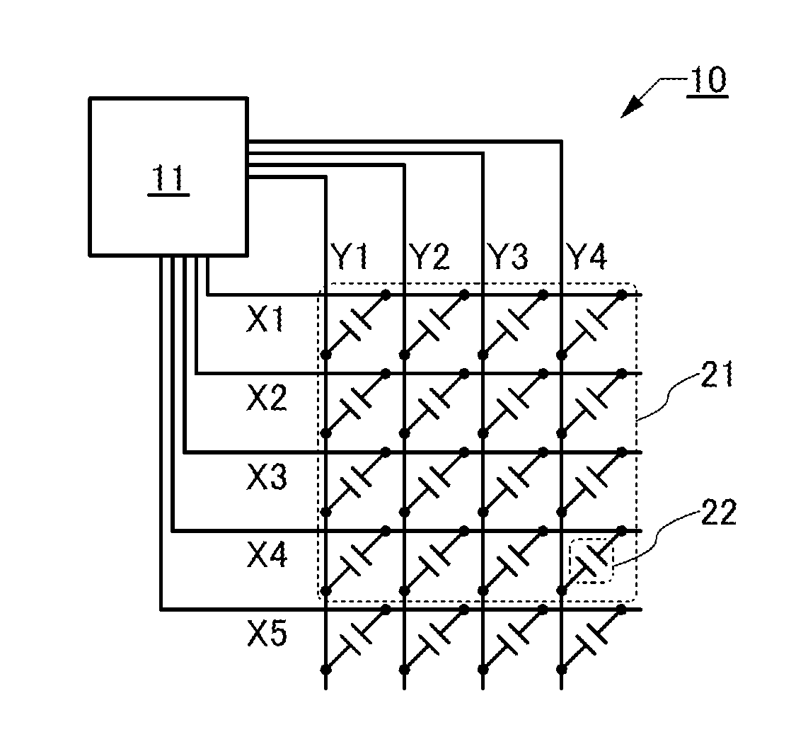
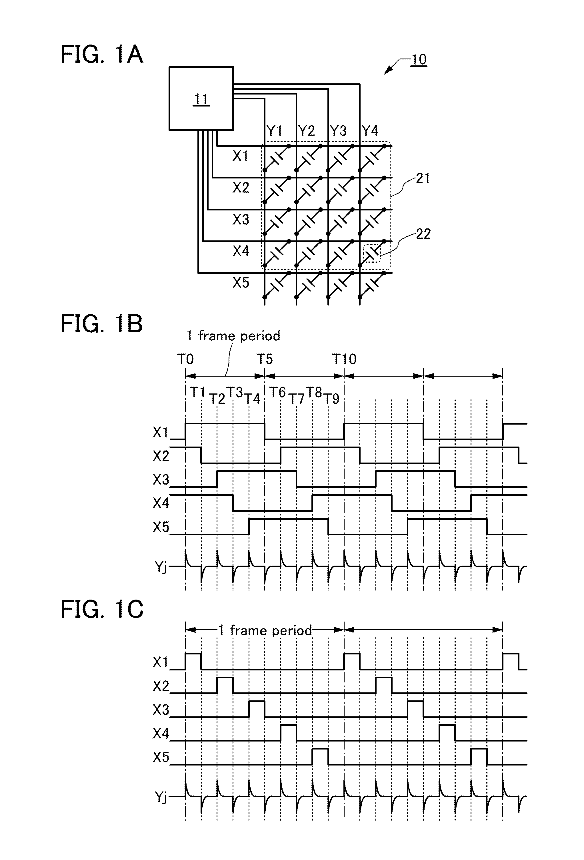
[0062]FIG. 1A illustrates a structure example of an input device 10. The input device 10 includes m (m is an integer of 2 or more) row wirings (row wirings X1 to Xm), n (n is an integer of 2 or more) column wirings (column wirings Y1 to Yn), and a circuit 11. The row wirings intersect the column wirings. A capacitor 22 is formed between one of the row wirings and one of the column wirings. The input device 10 includes a sensor array 21 in which a plurality of (m×n) capacitors 22 are arranged in a matrix.

[0063]For simplicity, FIG. 1A illustrates a structure of the input device 10 in which five row wirings (row wirings X1 to X5) and four column wirings (column wirings Y1 to Y4) are provided.

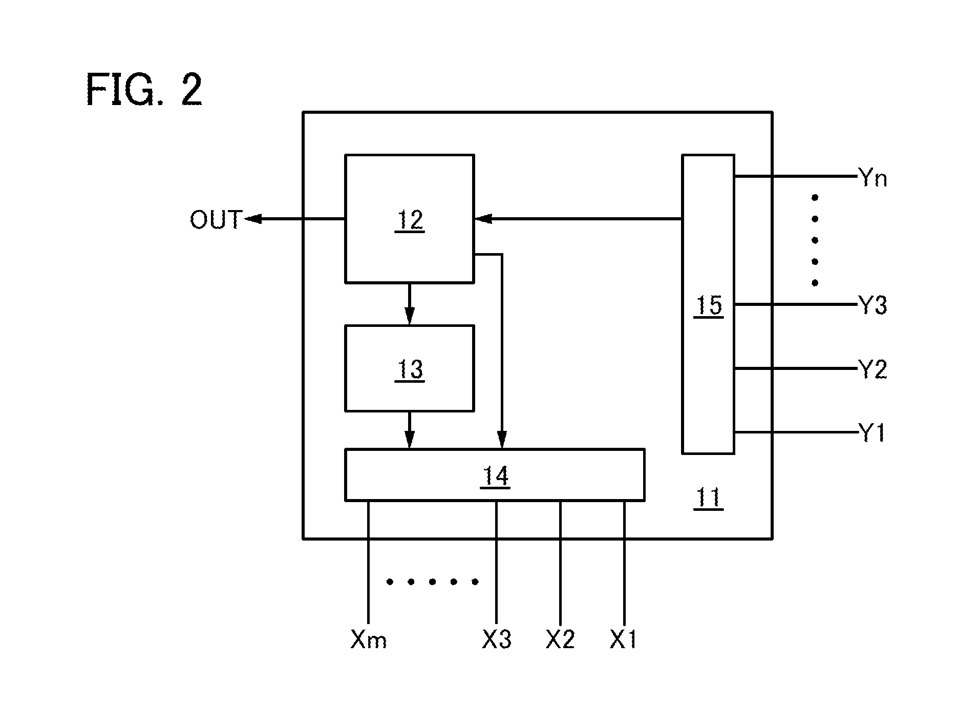
[0064]The circuit 11 has a function of out...

example 1

Cross-Sectional Structure Example 1

[0128]Next, an example of a cross-sectional structure of the touch panel 100 will be described with reference to a drawing. FIG. 11 is a schematic cross-sectional view of the touch panel 100. FIG. 11 illustrates cross sections of a region including the FPC 73, a region including the driver circuit 82, a region including the display portion 81, and a region including the FPC 50 in FIG. 10A.

[0129]The substrate 71 and the substrate 72 are attached to each other with an adhesive layer 151. The substrate72 and the substrate 30 are attached to each other with an adhesive layer 152. Here, a structure including the substrate 71, the substrate 72, and components provided therebetween corresponds to the display panel 70. A structure including the substrate 30 and components formed over the substrate 30 corresponds to the input device 10.

70>

[0130]The substrate 71 is provided with a transistor 201, a transistor 202, a transistor 203, a display element 204, a c...

modification example 1

of Cross-Sectional Structure Example

[0195]FIG. 12 illustrates a cross-sectional structure example of the touch panel 100 which partly differs from that in FIG. 11. Note that descriptions of the portions already described are omitted and different portions are described below.

[0196]In FIG. 12, in the transistors 201 and 202, conductive layers functioning as their second gates are provided between the insulating layer 213 and the insulating layer 214. Such a structure is preferable to the structure in FIG. 11 because the voltage to be applied to the second gates can be lowered.

[0197]FIG. 12 illustrates an example where the display element 204 is formed by a separate coloring method. Specifically, pixels for different colors include different EL layers 222 which emit light of the respective colors. In a region outside the light-emitting region of the display element 204, an end portion of the EL layer 222 is covered with the second electrode 223. The EL layer 222 can be formed by, for ...


PUM


Abstract

An input device or an input / output device that is suitable for increasing in size is provided. An input device or an input / output device that can be driven at high frequencies is provided. An input device includes a plurality of row wirings and a plurality of column wirings. To each of the plurality of row wirings, periodic rectangular waves are applied. When attention is paid to one row wiring Xi (i is greater than or equal to 1 and less than or equal to m−1), a signal that has a phase opposite to that of a signal applied to the row wiring Xi and that is delayed for a given period is applied to a row wiring Xi+1, which is the row wiring next to the row wiring Xi. The width of each of the rectangular waves applied to the row wirings corresponds to a frame period.

Description

BACKGROUND OF THE INVENTION[0001]1. Field of the Invention[0002]One embodiment of the present invention relates to an input device. One embodiment of the present invention relates to an input / output device.[0003]Note that one embodiment of the present invention is not limited to the above technical field. Examples of the technical field of one embodiment of the present invention disclosed in this specification include a semiconductor device, a display device, a light-emitting device, a power storage device, a memory device, an electronic device, a lighting device, an input device, an input / output device, a driving method thereof, and a manufacturing method thereof.[0004]In this specification and the like, a semiconductor device generally means a device that can function by utilizing semiconductor characteristics. A semiconductor element such as a transistor, a semiconductor circuit, an arithmetic device, and a memory device are each an embodiment of a semiconductor device. An imagin...

Claims


Application Information

Patent Timeline
Patent Type & Authority Applications(United States)
IPC IPC(8): G06F3/044G06F3/047
CPCG06F3/044G06F2203/04103G06F3/047B60K35/00G06F1/1626G06F1/163G06F1/1641G06F1/1652G06F3/0412G06F2203/04102G06F2203/04112B60K37/06B60K2370/143B60K2370/774B60K2370/794G06F3/04166G06F3/0446G06F3/03547G01R27/2605G02F1/13338G09G2320/0209H03K17/955
Inventor MIYAKE, HIROYUKI
Owner SEMICON ENERGY LAB CO LTD
Why Eureka
Try Eureka