Semiconductor apparatus

Inactive Publication Date: 2016-04-14
TOYOTA JIDOSHA KK
View PDF4 Cites 0 Cited by
  • Summary
  • Abstract
  • Description
  • Claims
  • Application Information

AI Technical Summary

Benefits of technology

[0007]An object of the present disclosure is to provide a semiconductor apparatus capable of

Problems solved by technology

Therefore, the surge voltage cannot be reduced easily when characteristics of the switching elements are not integrated.
However, integration of the characteristics of the switc

Method used


Image

  • Semiconductor apparatus
  • Semiconductor apparatus
  • Semiconductor apparatus

Examples


Example

[0019]In the following, embodiments are described in detail with reference to appended drawings.

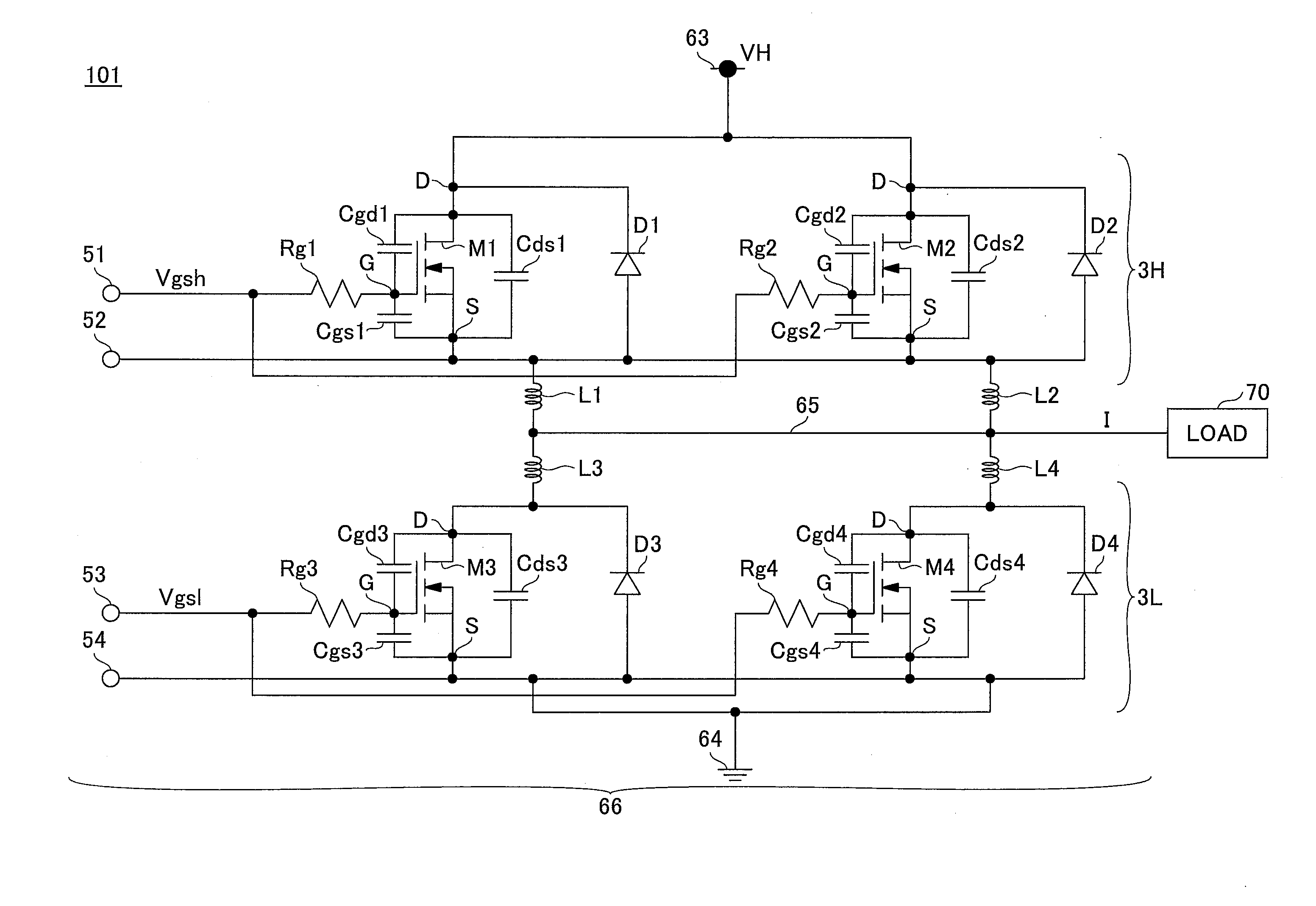
[0020]FIG. 1 is a diagram for illustrating an example configuration of a semiconductor apparatus of the present embodiment. The semiconductor apparatus of the present embodiment is an example of a semiconductor circuit including a driving unit for driving an inductive load 70 (such as an inductor or a motor) by turning on and off the switching elements.

[0021]A power conversion apparatus for converting input electric power into output electric power by switching on / off the switching elements is exemplified as an apparatus in which one or more of the semiconductor apparatuses are included. A converter for stepping-up or stepping-down DC voltage, an inverter for converting electric powers of DC power and AC power, etc., are exemplified as the power conversion apparatus.

[0022]In FIG. 1, an example of a power conversion apparatus 101 in which the semiconductor apparatuses are disposed at high ...


PUM


Abstract

There is provided a semiconductor apparatus comprising: a first switching element formed of a wide band gap semiconductor; and a second switching element formed of another wide band gap semiconductor and connected in parallel with the first switching element; wherein the first switching element and the second switching element respectively include a control electrode, a first main electrode and a second main electrode, and respectively have an output capacitance characteristic in which an output capacitance decreases as a voltage between the first main electrode and the second main electrode increases, and the output capacitance characteristics of the first switching element and the second switching element or threshold voltages for respectively turning on/off the first switching element and the second switching element are different from each other.

Description

BACKGROUND OF THE INVENTION[0001]1. Field of the Invention[0002]The present disclosure is related to a semiconductor apparatus including a switching element.[0003]2. Description of the Related Art[0004]A technology is known, in which a plurality of switching elements formed of silicon carbide are connected in parallel whereas signal transmissions to respective control nodes of the switching elements are shifted by wires connected with the respective control nodes, thereby reducing a surge voltage (for example, see Patent Document 1).[0005]In order to reduce the surge voltage with the aforementioned conventional technology, inductances of the respective wires are required to be set appropriately so as to shift timings of the signal transmissions to the respective control nodes. Therefore, the surge voltage cannot be reduced easily when characteristics of the switching elements are not integrated. However, integration of the characteristics of the switching elements is hardly achieved...

Claims


Application Information

Patent Timeline
IPC IPC(8): H01L27/02H01L27/088
CPCH01L27/088H01L27/0248H01L27/0255H03K17/122H03K17/163
Inventor YAMAMOTO, KAZUNARI
Owner TOYOTA JIDOSHA KK
Why Eureka
Try Eureka