Light-Emitting Element, Display Device, Electronic Device, and Lighting Device

a technology of light-emitting elements and electronic devices, which is applied in the direction of thermoelectric devices, planar light sources, lighting and heating apparatuses, etc., can solve the problems of difficult design of light-emitting materials that meet these two requirements, and achieve efficient excitation energy transfer, high fluorescence quantum yield, and increase the emission efficiency of light-emitting elements

Inactive Publication Date: 2016-04-14
SEMICON ENERGY LAB CO LTD
View PDF5 Cites 20 Cited by
  • Summary
  • Abstract
  • Description
  • Claims
  • Application Information

AI Technical Summary

Benefits of technology

[0012]In order to increase emission efficiency of a light-emitting element containing a thermally activated delayed fluorescent substance and a material emitting fluorescence, efficient generation of a singlet excited state from a triplet excited state in the thermally activated delayed fluorescent substance is important. Furthermore, efficient excitation energy transfer from the singlet excited state of the thermally activated delayed fluorescent substance to a singlet excited state of the material emitting fluorescence is important. In addition, efficient light emission from the singlet excited state of the material emitting fluorescence, that is, high fluorescence quantum yield of the material emitting fluorescence, is important.

Problems solved by technology

It is, however, difficult to design a light-emitting material that meets these two.

Method used


Image

  • Light-Emitting Element, Display Device, Electronic Device, and Lighting Device
  • Light-Emitting Element, Display Device, Electronic Device, and Lighting Device
  • Light-Emitting Element, Display Device, Electronic Device, and Lighting Device

Examples


embodiment 1

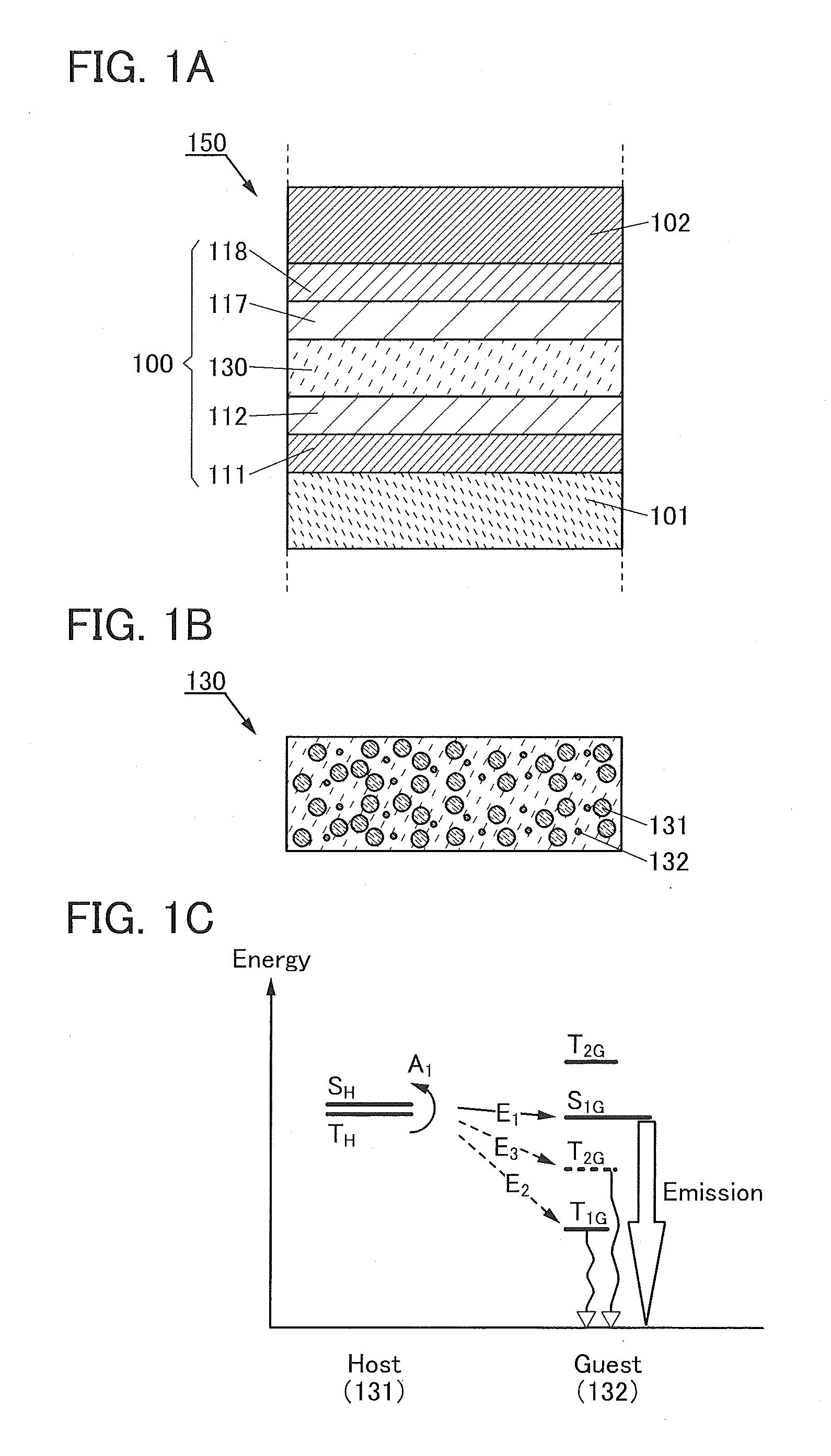
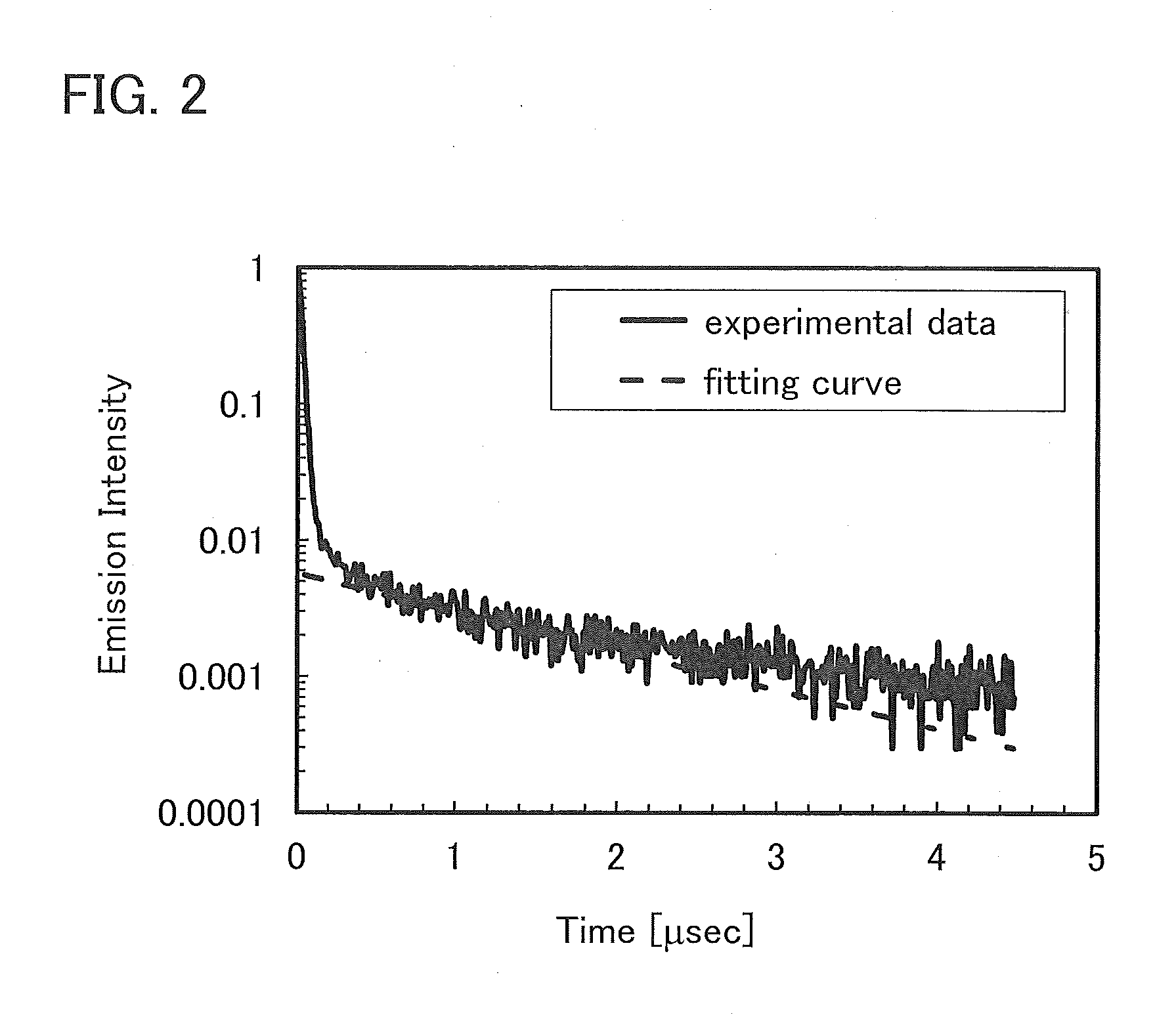
[0071]In this embodiment, a light-emitting element of one embodiment of the present invention will be described below with reference to FIGS. 1A to 1C, FIG. 2, and FIGS. 3A and 3B.

[0072]First, a structure of a light-emitting element of one embodiment of the present invention will be described below with reference to FIGS. 1A to 1C.

[0073]FIG. 1A is a schematic cross-sectional view of a light-emitting element 150 of one embodiment of the present invention.

[0074]The light-emitting element 150 includes an EL layer 100 between a pair of electrodes (an electrode 101 and an electrode 102). The EL layer 100 includes at least a light-emitting layer 130. Note that in this embodiment, description is given assuming that the electrode 101 and the electrode 102 serve as an anode and a cathode, respectively.

[0075]The EL layer 100 illustrated in FIG. 1A includes functional layers which are a hole-injection layer 111, a hole-transport layer 112, an electron-transport layer 117, and an electron-injec...

embodiment 2

[0209]In this embodiment, a light-emitting element having a structure different from that described in Embodiment 1 and an emission mechanism of the light-emitting element will be described below with reference to FIGS. 4A and 4B.

[0210]FIG. 4A is a schematic cross-sectional view of a light-emitting element 450.

[0211]The light-emitting element 450 illustrated in FIG. 4A includes a plurality of light-emitting units (in FIG. 4A, a light-emitting unit 441 and a light-emitting unit 442) between a pair of electrodes (an electrode 401 and an electrode 402). One light-emitting unit has the same structure as the EL layer 100 illustrated in FIG. 1A. That is, the light-emitting element 150 in FIG. 1A includes one light-emitting unit, while the light-emitting element 450 includes the plurality of light-emitting units. Note that the electrode 401 functions as an anode and the electrode 402 functions as a cathode in the following description of the light-emitting element 450; however, the functio...

embodiment 3

[0254]In this embodiment, a light-emitting element having a structure different from those described in Embodiment 1 and Embodiment 2 will be described below with reference to FIGS. 5A and 5B.

[0255]FIG. 5A is a schematic cross-sectional view of a light-emitting element 452 of one embodiment of the present invention.

[0256]The light-emitting element 452 includes a plurality of light-emitting units (in FIG. 5A, a light-emitting unit 446 and a light-emitting unit 447) between an electrode 401 and an electrode 402. One light-emitting unit has the same structure as the EL layer 100 illustrated in FIG. 1A. That is, the light-emitting element 150 in FIG. 1A includes one light-emitting unit, while the light-emitting element 452 includes the plurality of light-emitting units. Note that the electrode 401 functions as an anode and the electrode 402 functions as a cathode in the following description of this embodiment; however, the functions may be interchanged in the light-emitting element 452...


PUM

PropertyMeasurementUnit
triplet excitation energy levelaaaaaaaaaa
phosphorescence emission energyaaaaaaaaaa

Abstract

A light-emitting element including a fluorescent material as a light-emitting material and having high emission efficiency is provided. The light-emitting element includes a pair of electrodes and an EL layer provided between the pair of electrodes. The EL layer includes a host material and a guest material. The host material is capable of exhibiting thermally activated delayed fluorescence at room temperature. The guest material is capable of exhibiting fluorescence. The second triplet excitation energy level of the guest material is higher than or equal to the lowest singlet excitation energy level of the guest material.

Description

BACKGROUND OF THE INVENTION[0001]1. Field of the Invention[0002]One embodiment of the present invention relates to a light-emitting element in which a light-emitting layer capable of providing light emission by application of an electric field is provided between a pair of electrodes, and also relates to a display device, an electronic device, and a lighting device including the light-emitting element.[0003]Note that one embodiment of the present invention is not limited to the above technical field. The technical field of one embodiment of the invention disclosed in this specification and the like relates to an object, a method, or a manufacturing method. In addition, one embodiment of the present invention relates to a process, a machine, manufacture, or a composition of matter. Specifically, examples of the technical field of one embodiment of the present invention disclosed in this specification include a semiconductor device, a display device, a liquid crystal display device, a...

Claims


Application Information

Patent Timeline
Patent Type & Authority Applications(United States)
IPC IPC(8): H01L51/50H01L51/52H01L27/32
CPCH01L51/5016H01L27/3244H01L27/322H01L27/323H01L51/5237H01L2251/5376H01L51/0067H01L51/0058H01L51/0072H01L51/006H01L51/0054H01L51/0055H01L2251/5384H10K50/121H10K50/11H10K2101/10H10K2101/27H10K2101/90H10K2101/30H10K2101/20H10K59/38H10K59/40H10K50/12C09K11/06C07C15/28C09K2211/1003F21Y2105/00H10K85/615
Inventor OHSAWA, NOBUHARUSEO, SATOSHI
Owner SEMICON ENERGY LAB CO LTD
Why Eureka
Try Eureka