Integrated circuits with laterally diffused metal oxide semiconductor structures and methods for fabricating the same

Active Publication Date: 2016-04-21
GLOBALFOUNDRIES SINGAPORE PTE LTD
View PDF4 Cites 31 Cited by
  • Summary
  • Abstract
  • Description
  • Claims
  • Application Information

AI Technical Summary

Benefits of technology

[0007]Integrated circuits with improved laterally diffused metal oxide semiconductor (LDMOS) structures, and methods for fabricating the same, are provided. In one embodiment, an exemplary LDMOS integrated circuit includes an n-type reduced surface field region, a p-type body well disposed on a lateral side of the n-type reduced surface fiel

Problems solved by technology

While useful in many applications, LDMOS devices are not without drawbacks.
For example, “hot carrier injection” (HCI) degradation can significantly limit the performance of these devices.
This injection of charge carriers often results in a localized and non-uniform buildup of interface states and oxide charges near and underneath a gate and/or in the drift region of the device.
For example, HCI can produce variations in certain characteristics of the LDMOS device, including saturation current, threshold voltage, transconductance, on-resistance, etc., thus undesirably affecting the performance and reliability of the device.
Locating the LDD region in close relative proximity to the silicon/oxide interface, however, significantly increases the li

Method used


Image

  • Integrated circuits with laterally diffused metal oxide semiconductor structures and methods for fabricating the same
  • Integrated circuits with laterally diffused metal oxide semiconductor structures and methods for fabricating the same
  • Integrated circuits with laterally diffused metal oxide semiconductor structures and methods for fabricating the same

Examples


Example

[0016]The following detailed description is merely exemplary in nature and is not intended to limit the various embodiments or the application and uses thereof. Furthermore, there is no intention to be bound by any theory presented in the preceding background or the following detailed description.

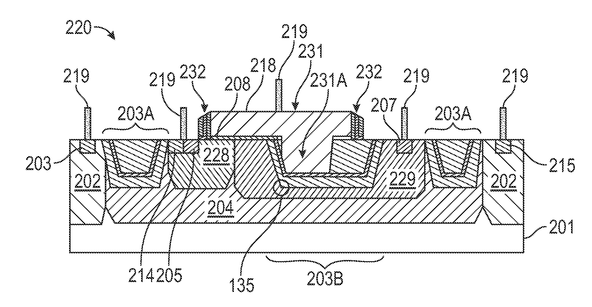
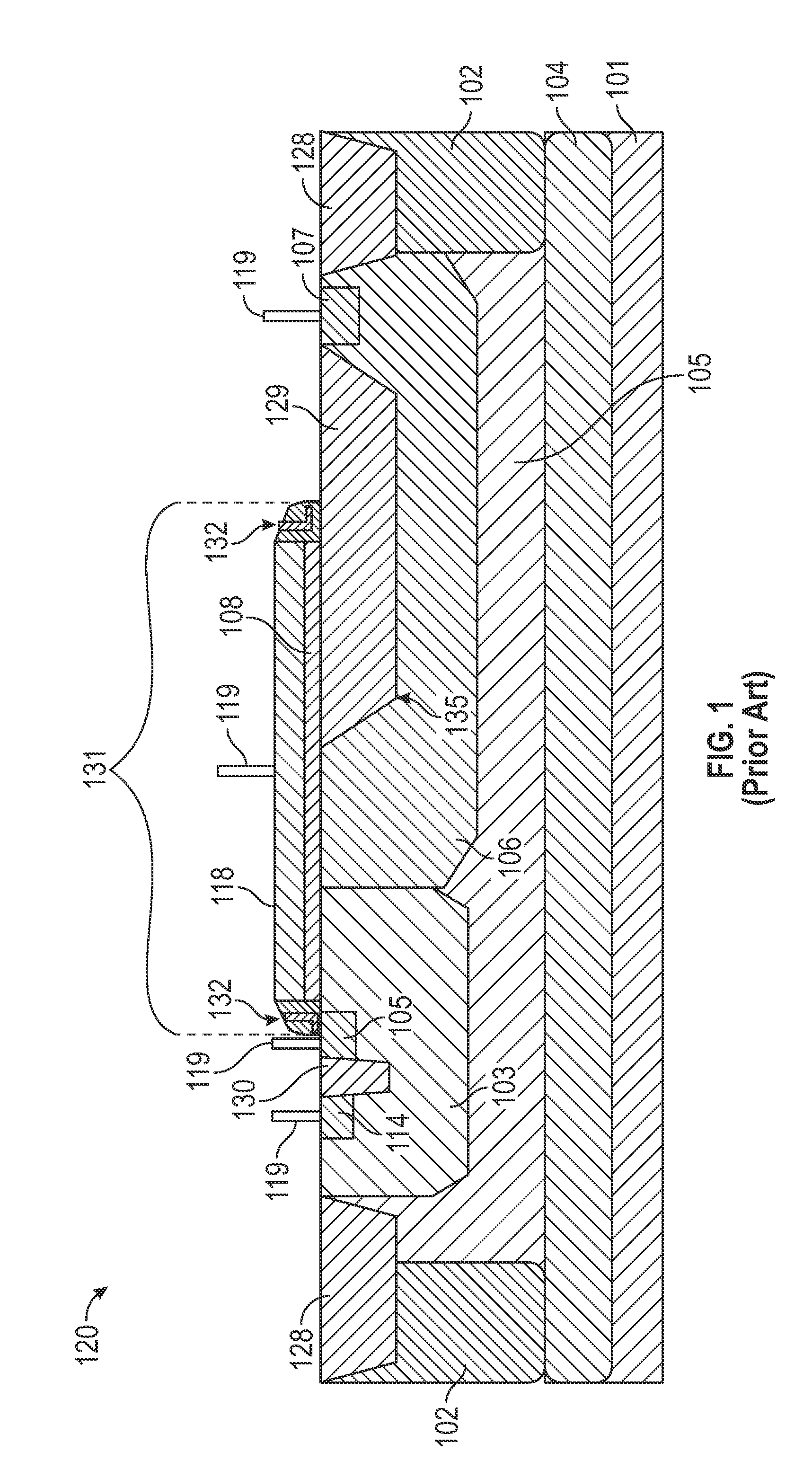
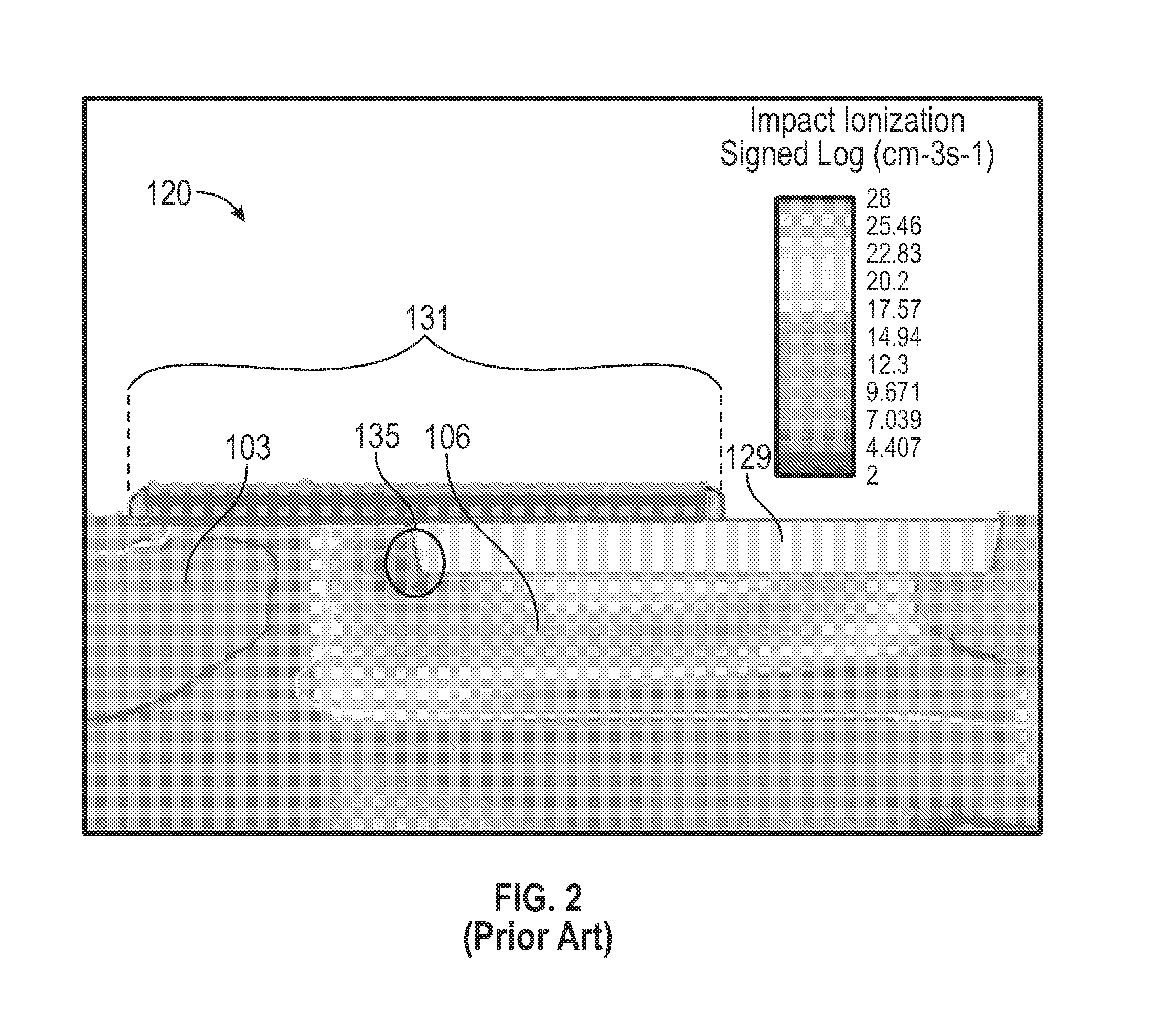
[0017]Various embodiments of LDMOS integrated circuits, and method for fabricating the same, are described herein. The described embodiments utilize an extended gate region within the shallow isolation trench structure located under the transistor gate electrode, in contrast with the conventional approach of using a shallow trench isolation structure with no gate extension therein, as will be described in greater detail below. The described embodiments reduce the impact of the HCI phenomenon, thereby allowing the LDMOS integrated circuits to be operated at more desirable voltage and current levels. Further, the described embodiments reduce fabrications cost and complexities for LDMOS integr...


PUM


Abstract

Integrated circuits with improved laterally diffused metal oxide semiconductor (LDMOS) structures, and methods of fabricating the same, are provided. An exemplary LDMOS integrated circuit includes an n-type reduced surface field, a p-type body well disposed on a lateral side of the n-type reduced surface field region, a shallow trench isolation structure disposed within the n-type reduced surface field region, and a gate structure disposed partially over the p-type body well, partially over the n-type reduced surface field region, partially over the shallow trench isolation structure, and partially within the shallow trench isolation structure.

Description

TECHNICAL FIELD[0001]The technical field generally relates to integrated circuits and methods for fabricating integrated circuits, and more particularly relates to laterally diffused metal oxide semiconductor (LDMOS) integrated circuit structures and methods for fabricating the same.BACKGROUND[0002]The majority of present day integrated circuits are implemented by using a plurality of interconnected field effect transistors (FETs), also called metal oxide semiconductor field effect transistors (MOSFETs), or simply MOS transistors. A MOS transistor includes a gate electrode as a control electrode and spaced apart source and drain regions between which a current can flow. A control voltage applied to the gate electrode controls the flow of current through an underlying channel between the source and drain regions.[0003]Power MOS devices, including lateral diffused MOS (LDMOS) devices, are employed in a wide variety of applications, such as, for example, power amplifiers in wireless co...

Claims


Application Information

Patent Timeline
IPC IPC(8): H01L29/06H01L21/762H01L29/423H01L21/311H01L21/28H01L29/66H01L29/78H01L21/02
CPCH01L29/063H01L29/7823H01L29/7825H01L29/0653H01L21/76224H01L29/4236H01L21/0217H01L21/31111H01L21/28035H01L29/66704H01L21/02164H01L29/42368H01L29/1087H01L21/76229H01L21/76232H01L29/407
Inventor LU, YIWANG, DONGLICHEN, DEYANVERMA, PURAKH RAJ
Owner GLOBALFOUNDRIES SINGAPORE PTE LTD
Why Eureka
Try Eureka