Organic light emitting device and method of fabricating the same

a light emitting device and organic technology, applied in the direction of thermoelectric device junction materials, semiconductor devices, electrical equipment, etc., can solve the problems of increasing reducing reliability, and limiting the current (a) per unit area so as to improve the quality and productivity of the oled display, enhance the efficiency and lifetime and reduce the power consumption of the organic light emitting devi

Active Publication Date: 2016-05-05
LG DISPLAY CO LTD
View PDF6 Cites 16 Cited by
  • Summary
  • Abstract
  • Description
  • Claims
  • Application Information

AI Technical Summary

Benefits of technology

[0016]Various structures of an organic light emitting device for enhancing efficiency and lifetime of the organic light emitting device and reducing power consumption of the organic light emitting device have been proposed to improve quality and productivity of an OLED display.

Problems solved by technology

However, the OLED display has a limit on current (A) per unit area due to the emission structure of the OLED display.
In addition, increasing the current applied to the organic light emitting device leads to lower reliability and increased power consumption of the organic light emitting device.
As the organic emission layers are formed using the FMM as above, the fabrication process of the organic light emitting device becomes complex and productivity of the organic light emitting device is lowered.
Due to the thickness of the red EML 135 of the red sub-pixel area Rp formed as above, the driving voltage of the organic light emitting device 100 significantly increases along with an increase in power consumption.
The mask rib leads to a poor organic light emitting device.

Method used


Image

  • Organic light emitting device and method of fabricating the same
  • Organic light emitting device and method of fabricating the same
  • Organic light emitting device and method of fabricating the same

Examples


Embodiment Construction

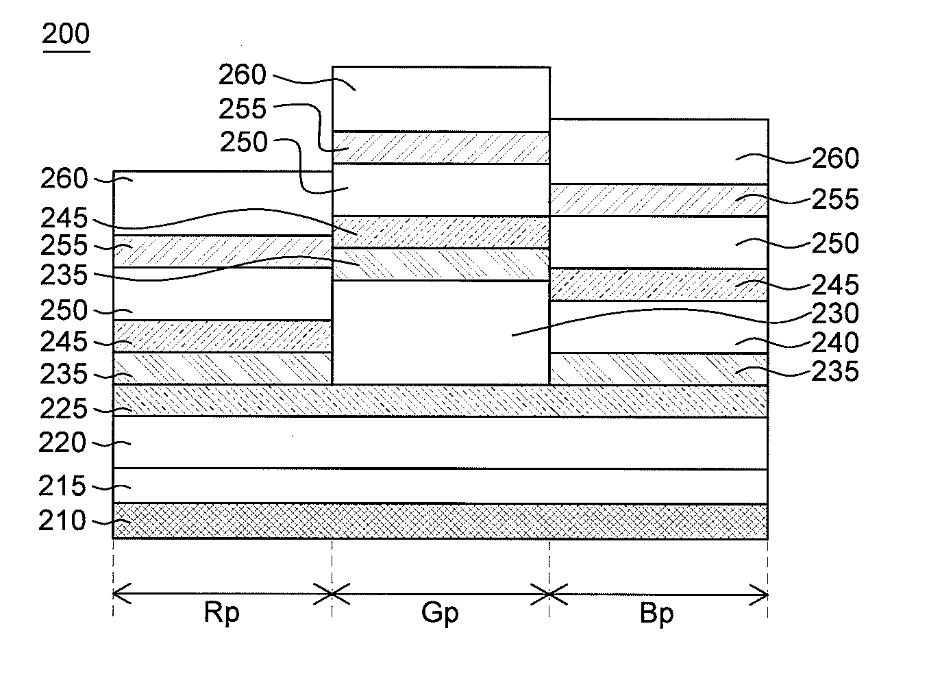
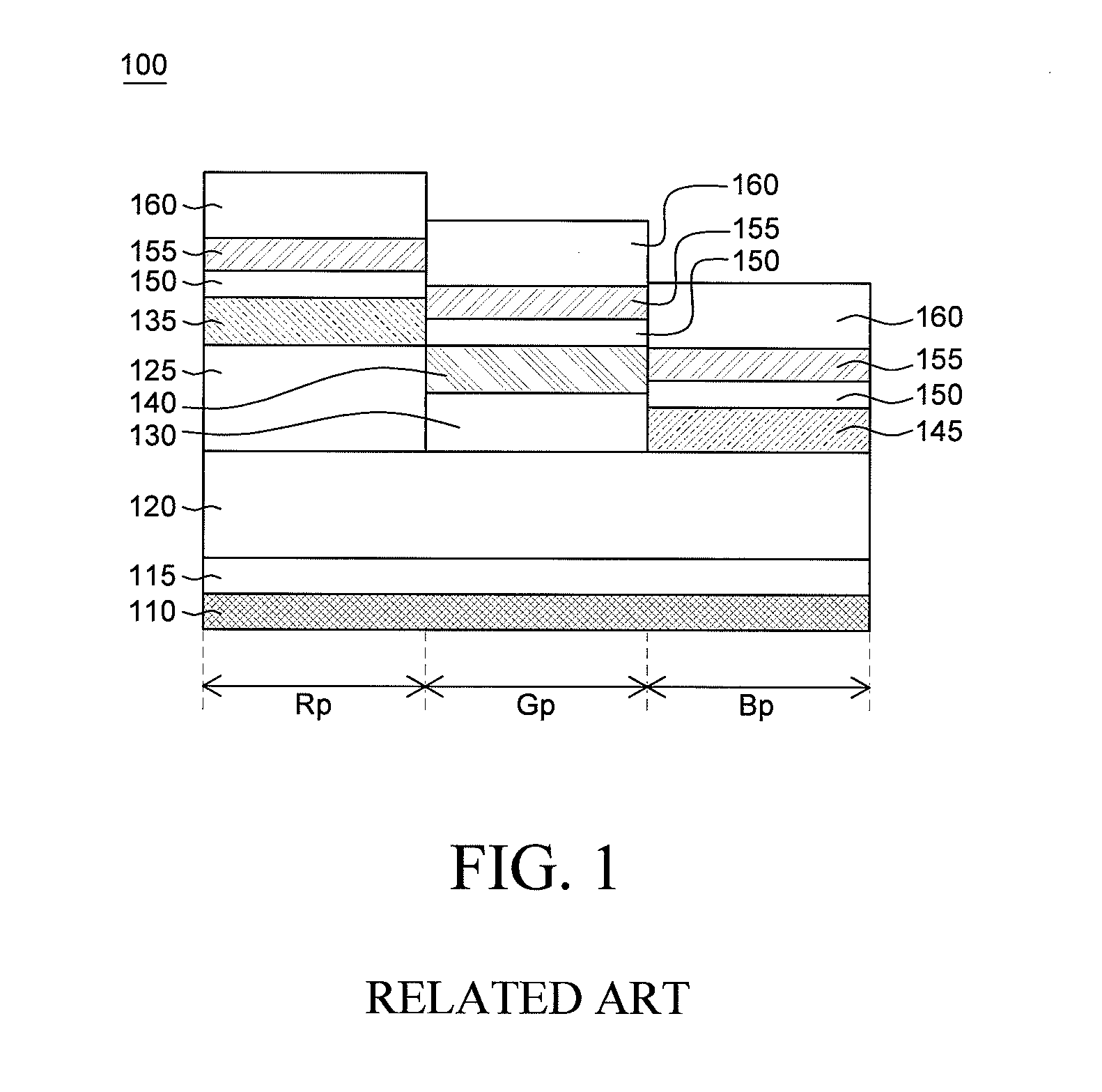
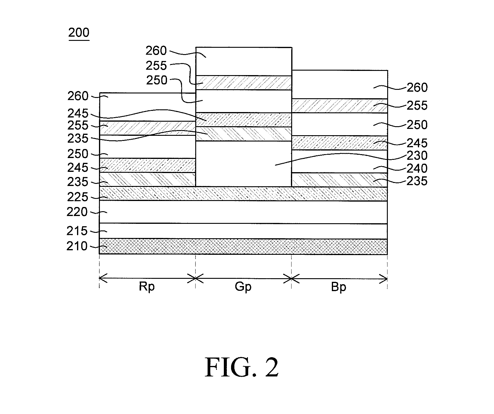
[0054]Advantages and features of the present invention and methods to achieve them will become apparent from the descriptions of embodiments herein below with reference to the accompanying drawings. However, the present invention is not limited to embodiments disclosed herein but may be implemented in various different forms. The embodiments are provided for making the disclosure of the present invention thorough and for fully conveying the scope of the present invention to those skilled in the art. It is to be noted that the scope of the present invention is defined only by the claims.

[0055]The figures, dimensions, ratios, angles, numbers of elements given in the drawings are merely illustrative and are not limiting. Like reference numerals denote like elements throughout the descriptions. Further, in describing the present invention, descriptions on well-known technologies may be omitted in order not to obscure the gist of the present invention. It is to be noticed that the terms ...


PUM


Abstract

An organic light emitting device can include a first electrode and a second electrode, and a red emission layer, a green emission layer and a blue emission layer which are positioned between the first electrode and the second electrode. Each of the red emission layer, the green emission layer and the blue emission layer can be disposed in an entirety of a red sub-pixel area, a green sub-pixel area and a blue sub-pixel area. A distance between the first electrode and the second electrode in at least one of the red sub-pixel area, the green sub-pixel area and the blue sub-pixel area can be a first-order optical distance equal to λ/2n, where λ is a wavelength of light emitted from each of the sub-pixel areas, and n is an average refractive index of a plurality of organic material layers disposed between the first electrode and the second electrode.

Description

CROSS-REFERENCE TO RELATED APPLICATIONS[0001]This application claims the priority of Patent Application No. 10-2014-0150304 filed on Oct. 31, 2014, in the Republic of Korea, the disclosure of which is incorporated herein by reference.BACKGROUND OF THE INVENTION[0002]1. Field of the Invention[0003]Embodiments of the present invention relate to an organic light emitting device and, more particularly, to an organic light emitting device capable of simplifying a manufacturing process, enhancing efficiency and reducing power consumption, and a method of fabricating the same.[0004]2. Description of the Related Art[0005]An organic light emitting diode (OLED) display is a self-luminous display employing an organic light emitting device. The organic light emitting device has an emission layer between an a cathode serving as an electron injection electrode and an anode serving as a hole injection electrode. The organic light emitting device receives electrons from the cathode and holes from t...

Claims


Application Information

Patent Timeline
Patent Type & Authority Applications(United States)
IPC IPC(8): H01L27/32H01L51/52
CPCH01L27/3218H01L51/5262H01L2227/323H01L51/5096H01L51/5088H01L51/5056H10K50/13H10K50/11H10K2101/10H10K71/00H10K59/30H10K59/35H10K50/852H10K50/131H10K50/15H10K50/16H10K50/17H10K50/18H10K50/155
Inventor KIM, MINA
Owner LG DISPLAY CO LTD
Why Eureka
Try Eureka