Method for forming vias on printed circuit boards

a technology of printed circuit boards and vias, which is applied in the direction of printed circuit manufacturing, printed circuit aspects, printed element electric connection formation, etc., can solve the problems of difficult placement of electrical components, time and complexity, and disadvantages of leaving via holes without some type of filling, and achieve high conductivity.

Inactive Publication Date: 2016-05-05
NCC NANO LLC
View PDF3 Cites 18 Cited by
  • Summary
  • Abstract
  • Description
  • Claims
  • Application Information

AI Technical Summary

Benefits of technology

[0028]Among advantages provided by embodiments of the present disclosure is the ability rapidly fill and sinter vias. By utilizing oven sintering methods, vias of all types, including through vias and blind vias, can be filled and sintered. The use of the specified conductive pastes ensures high levels

Problems solved by technology

It can be disadvantageous to leave the via hole without some type of filling, however.
A simple unfilled via leaves a perforation or hole in the circuit board upon which it is difficult to place an electrical component.
Electroplating is one approach that is commonly used for this purpose, but can be costly in terms of time and complexity.
The electroplating process requires harsh chemical baths with consequent handling of toxic materials.
The cost of epoxy-based via fill materials is relatively high, due in part to the silver content.
Pastes of this type generally have a relatively shor

Method used


Image

  • Method for forming vias on printed circuit boards
  • Method for forming vias on printed circuit boards
  • Method for forming vias on printed circuit boards

Examples


example

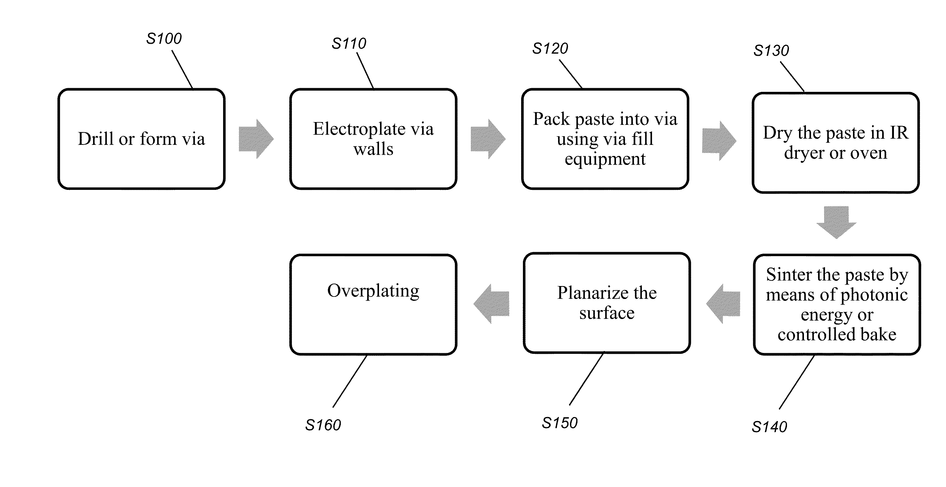
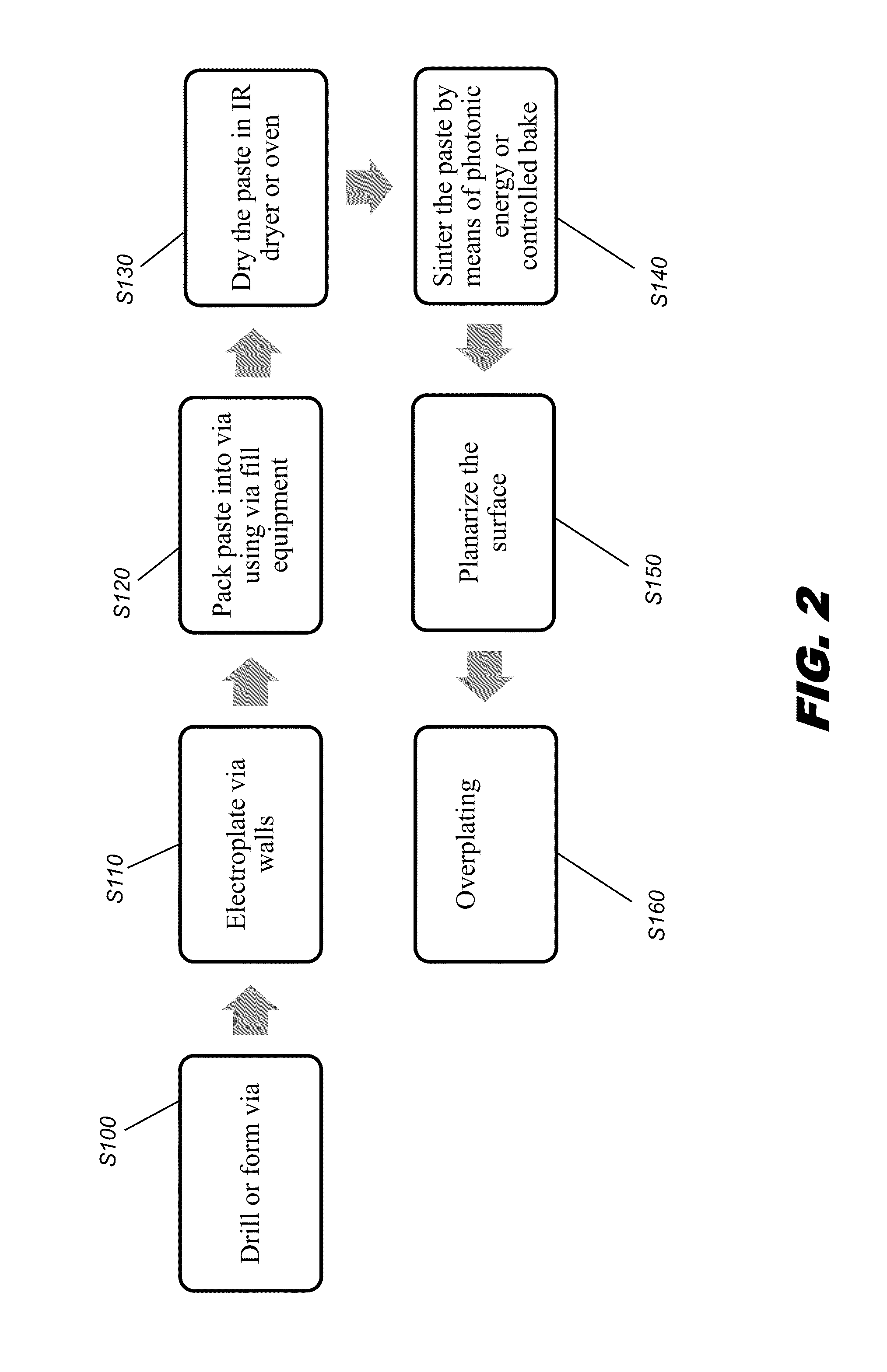
[0090]According to an embodiment of the present disclosure, PCBs having a number of vias were prepared and processed using the methods described hereinabove.

[0091]The via fill material was a paste having copper nanoparticle and micron-sized particulate in the ratio of 1:1, with copper loading of 70% nominal by weight, in a solvent that includes A-Terpineol, approximately 25% by weight, with polyvinyl butyral as an organic binder.

[0092]The vias on the PCB were filled using a squeegee blade and dried in a vacuum oven at a nominal temperature of about 50 degrees C. for one hour. The PCB was then sintered in an oven at temperatures ranging from about 190 to 225 degrees C. for one hour under a reducing environment. The filled vias were then planarized, and overplated with copper using non-electroless plating.

[0093]An IPC solder float test was performed on finished over-plated vias. The float test was executed over 5 cycles, with 10 seconds at 550 degrees F., allowed to cool to ambient be...


PUM

PropertyMeasurementUnit
Fractionaaaaaaaaaa
Fractionaaaaaaaaaa
Fractionaaaaaaaaaa

Abstract

A method for filling a via on a printed circuit board formulates a paste as a dispersion of copper particulate that includes nanocopper particles in a solvent and a binder and depositing the paste into a via cavity formed in the printed circuit board. Heating the paste-filled cavity removes most of the solvent. The method sinters the deposited paste in the via cavity, planarizes the sintered via, and overplates the filled via with copper.

Description

CROSS REFERENCE TO RELATED APPLICATIONS[0001]This patent application claims the benefit of priority to U.S. Provisional Patent Application Ser. No. 62 / 074687, entitled “A METHOD FOR FORMING VIAS ON PRINTED CIRCUIT BOARDS” filed on Nov. 4, 2014 in the names of David Ciufo and Janet Heyen which is hereby incorporated by reference herein in its entirety.FIELD OF THE INVENTION[0002]This invention relates in general to forming vias for circuit boards and more particularly relates to apparatus and methods for depositing electronic paste into a via cavity and sintering the deposited material to form a filled conductive via.BACKGROUND[0003]Fabrication of mass-produced electronic items such as printed circuit boards (PCBs) typically involves utilizing both sides of the circuit board as well as using one or more internal layers within a laminated stack of integrated circuit boards. The opposite sides, internal layers, and adjacent stacked boards are electrically connected by means of vias. Vi...

Claims


Application Information

Patent Timeline
IPC IPC(8): H05K3/00H05K3/42
CPCH05K3/0094H05K3/429H05K3/0047H05K3/4069H05K1/0306H05K1/032H05K1/097H05K3/1233H05K3/227H05K3/26H05K3/4617H05K2201/0266H05K2201/0347H05K2201/09509H05K2201/09536H05K2201/09563H05K2203/0139H05K2203/085H05K2203/086H05K2203/107H05K2203/1131H05K2203/143H05K2203/1438Y10T29/49165
Inventor CIUFO, DAVIDHEYEN, JANET
Owner NCC NANO LLC
Why Eureka
Try Eureka