
Method and Apparatus for Monitoring Pulsed Plasma Processes

a pulsed plasma and process technology, applied in the field of optical emission spectroscopy, can solve the problems that the light emission from pulsed plasma generated by rf plasma reactors may also exhibit light variations, and achieve the effect of reducing random intensity variation

Inactive Publication Date: 2016-05-12
VERITY INSTR
View PDF2 Cites 11 Cited by
  • Summary
  • Abstract
  • Description
  • Claims
  • Application Information

AI Technical Summary

Benefits of technology

The present invention is about a system, method, and software product for monitoring a pulsed plasma wafer processing system. It detects, amplifies, and digitizes the light emitted from the system and creates a stable local reference waveform signal by combining the digitized signals from each RF modulation period. This reference waveform signal is then compared to the instantaneous waveform signals from the pulsed plasma system or used for signal processing techniques like Fourier analysis. The technical effect of this invention is the creation of a reliable and stable reference waveform signal that can help improve the accuracy and consistency of plasma processing.

Problems solved by technology

However, the light emission from a pulsed plasma generated by an RF plasma reactor may also exhibit light variations at time scales comparable to the RF modulation period of the pulsed plasma that are not detectable using conventional OES techniques.

Method used


Image

  • Method and Apparatus for Monitoring Pulsed Plasma Processes
  • Method and Apparatus for Monitoring Pulsed Plasma Processes
  • Method and Apparatus for Monitoring Pulsed Plasma Processes

Examples


Embodiment Construction

Element Reference Number Designations

[0016]

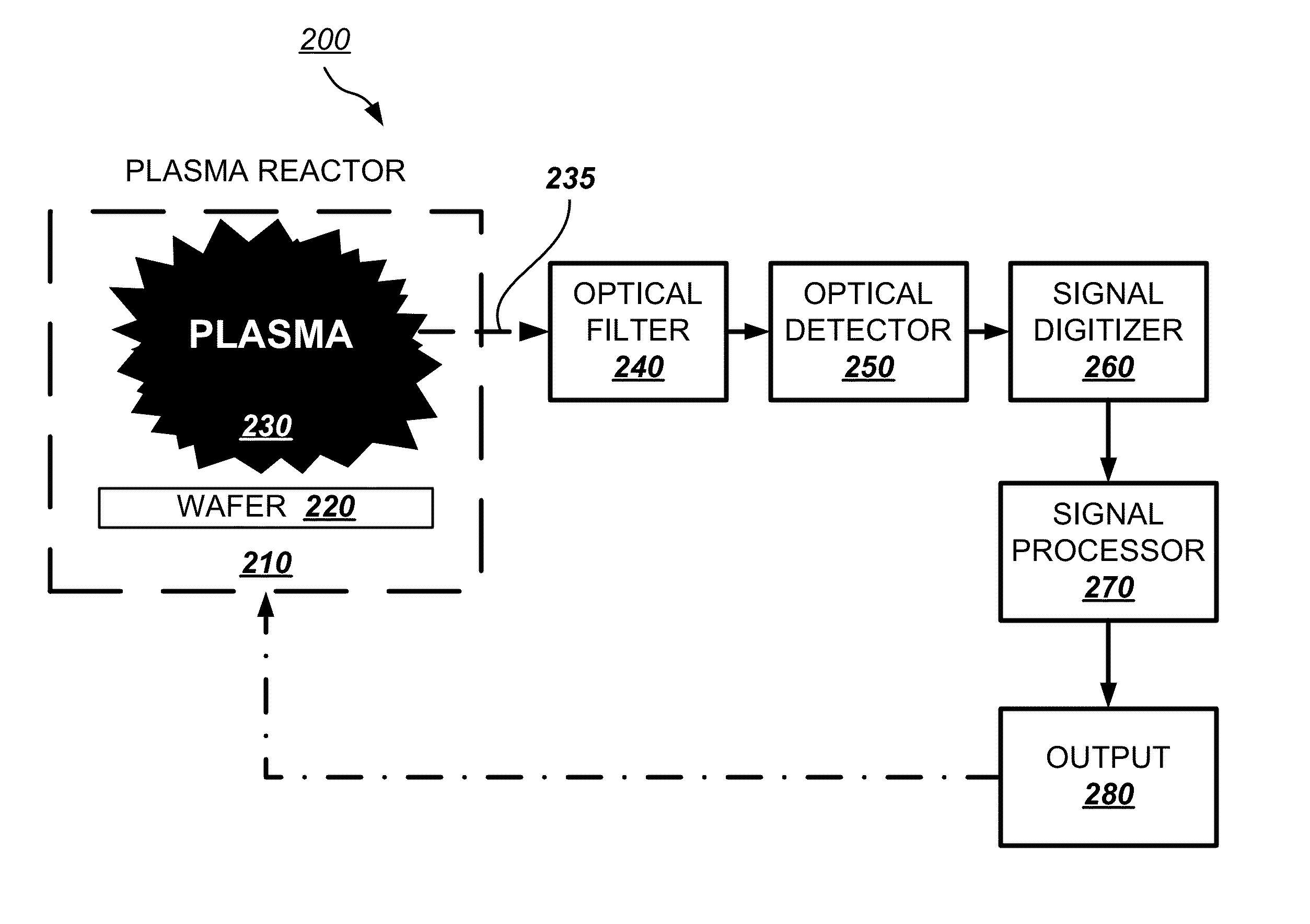
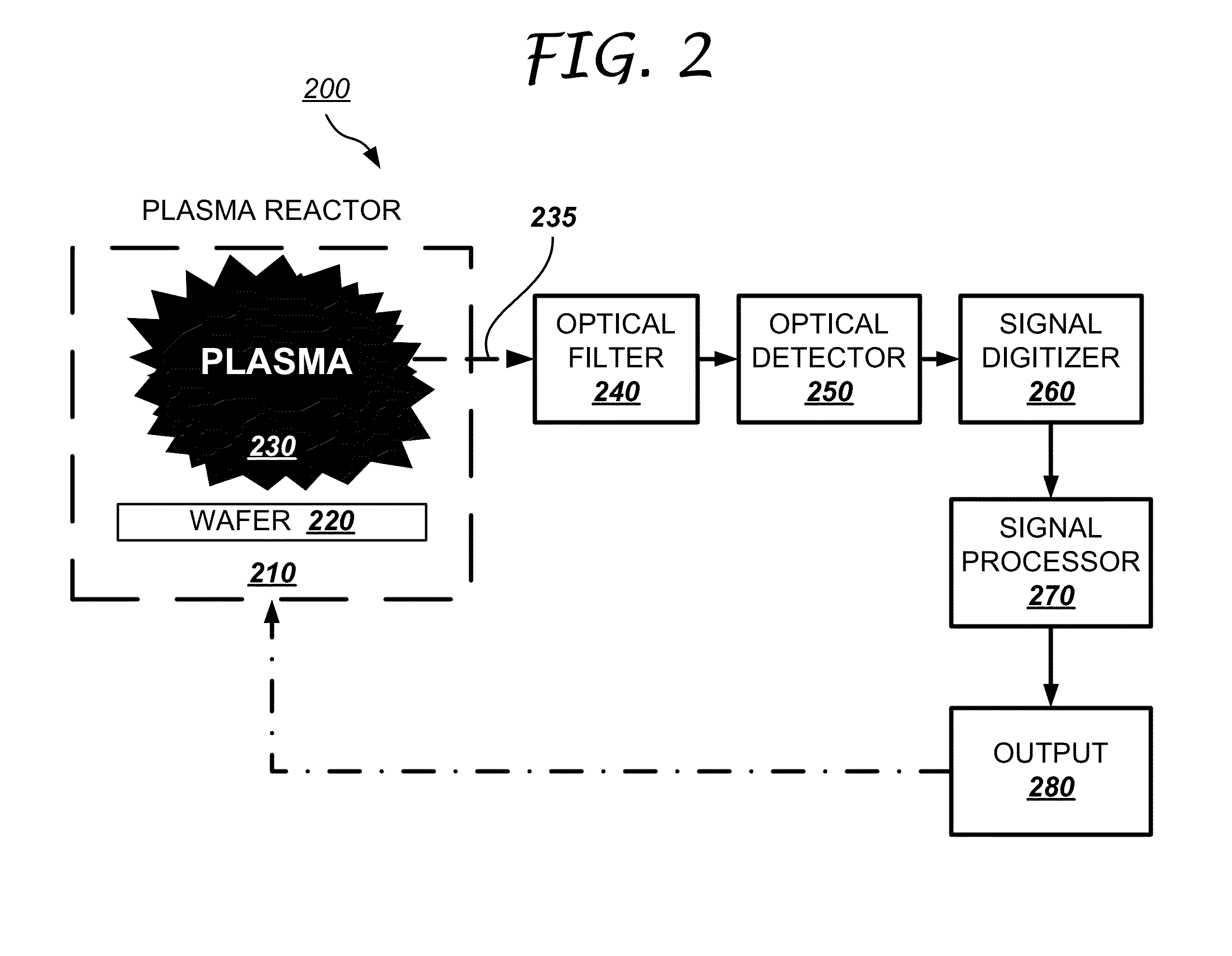
200: Pulsed plasma monitoring system210: Plasma reactor220: Wafer230: Plasma235: Emitted light240: Optical filter250: Optical Detector260: Signal Digitizer270: Signal Processor280: Output800: Pulsed plasma monitoring system810: Separable processor subsystem820: Detector subsystem830: Interface cable840: Fiber optic adapter850: Display860: Power switch870: Power connector880: Communication interface

[0017]In the following description, reference is made to the accompanying drawings that form a part hereof, and in which is shown by way of illustration, specific embodiments in which the invention may be practiced. These embodiments are described in sufficient detail to enable those skilled in the art to practice the invention, and it is to be understood that other embodiments may be utilized. It is also to be understood that structural, procedural and system changes may be made without departing from the spirit and scope of the present invention...


PUM

PropertyMeasurementUnit
RF frequencyaaaaaaaaaa
frequencyaaaaaaaaaa
frequencyaaaaaaaaaa

Abstract

Emitted light from a pulsed plasma system is detected, amplified and digitized over a plurality of pulse modulation cycles to produce a digitized signal over the plurality of RF modulation periods, each of which contains an amount of random intensity variations. The individual signal periods are then mathematically combined to produce a stable local reference waveform signal that has decreased random intensity variations. One mechanism for creating a stable local reference waveform signal is by subdividing each of the individual signal periods into a plurality of subunits and the mathematically averaging the respective subunits within the modulation period to produce the stable local reference waveform signal for the modulation period. The stable local reference waveform signal can then be compared to other instantaneous waveform signals from the pulsed plasma system, or waveform parameters can be derived using various signal processing techniques such as Fourier analysis.

Description

CROSS-REFERENCE TO RELATED APPLICATIONS[0001]The present application is related to and claims priority from co-pending U.S. Provisional Patent Application Ser. No.: 62 / 043,215, which is assigned to the assignee of the present invention. The above identified application is incorporated by reference herein in its entirety.BACKGROUND OF THE INVENTION[0002]The present invention relates generally to optical emission spectroscopy. More particularly, the present invention relates to a system, method and software program product for monitoring and analyzing the optical emission from a pulsed plasma wafer processing system.[0003]Optical emission spectroscopy (OES) is widely used in the semiconductor industry for monitoring the state of a wafer process within a reactor by using the plasma light emission generated within the reactor. While OES techniques may vary with the particular application and process, typically the light emission intensities are monitored at one or more predetermined wav...

Claims


Application Information

Patent Timeline
Patent Type & Authority Applications(United States)
IPC IPC(8): G01N21/66H01J37/32
CPCG01N21/66H01J37/321G01N2201/12H01J37/32137H01J37/32174G01N21/68G01N2021/8416H01J37/32082H01J37/32146H01J37/32926H01J37/32935H01J37/32972H01J37/3299
Inventor MELONI, MARK ANTHONYKUENY, ANDREW WEEKSBULLOCK, LARRY ARLOSMICHALS, TIM CHARLESPYLANT, CHRISTOPHER DAVID
Owner VERITY INSTR
Learn More