Optical transceiver outputting wavelength multiplexed signal and receiving another wavelength multiplexed signal

a transceiver and wavelength multiplexing technology, applied in the field of optical transceivers, can solve problems such as degrading the sensitivity of optical receivers

Active Publication Date: 2016-05-26
SUMITOMO ELECTRIC IND LTD
View PDF6 Cites 14 Cited by
  • Summary
  • Abstract
  • Description
  • Claims
  • Application Information

AI Technical Summary

Problems solved by technology

Thus, the signal line for the optical transmitter may cause an EMI noise source against the signal line for the optical receiver, which degrades the sensitivity of the optical receiver.

Method used


Image

  • Optical transceiver outputting wavelength multiplexed signal and receiving another wavelength multiplexed signal
  • Optical transceiver outputting wavelength multiplexed signal and receiving another wavelength multiplexed signal
  • Optical transceiver outputting wavelength multiplexed signal and receiving another wavelength multiplexed signal

Examples


first embodiment

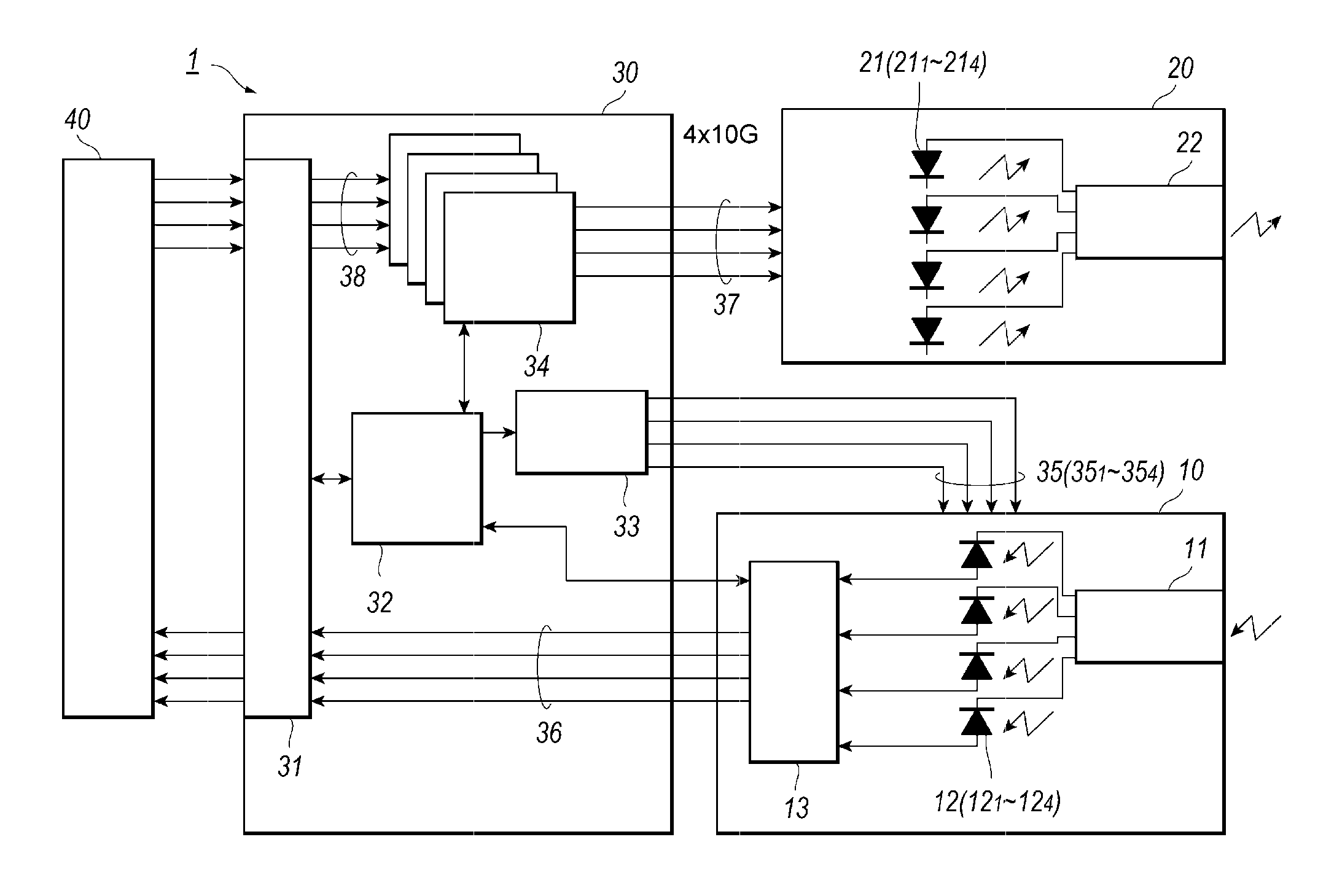
[0015]FIG. 1 shows a functional block diagram of an optical transceiver according to an embodiment of the present application. The optical transceiver 1, which is a type of a pluggable optical transceiver plugged with a host system, shows transmission capacity of 40 Gbps by wavelength multiplexing four (4) optical signals having respective wavelengths different from each other in a range of 1.3 μm. The description below concentrates on an optical transceiver of 40 Gbps, but the same description may be applicable to another type of an optical transceiver having, for instance, 100 Gbps transmission speed. Specifications including outer dimensions and electrical interfaces are defined by a multi-source agreements (MSAs) called as QSFP+ (Quad Small From factor Pluggable) or CFP (Centum Form factor Pluggable).

[0016]The optical transceiver 1 includes an optical receiver module (hereinafter denoted as Rx module) 10, an optical transmitter module (hereinafter denoted as Tx module) 20, and a...

second embodiment

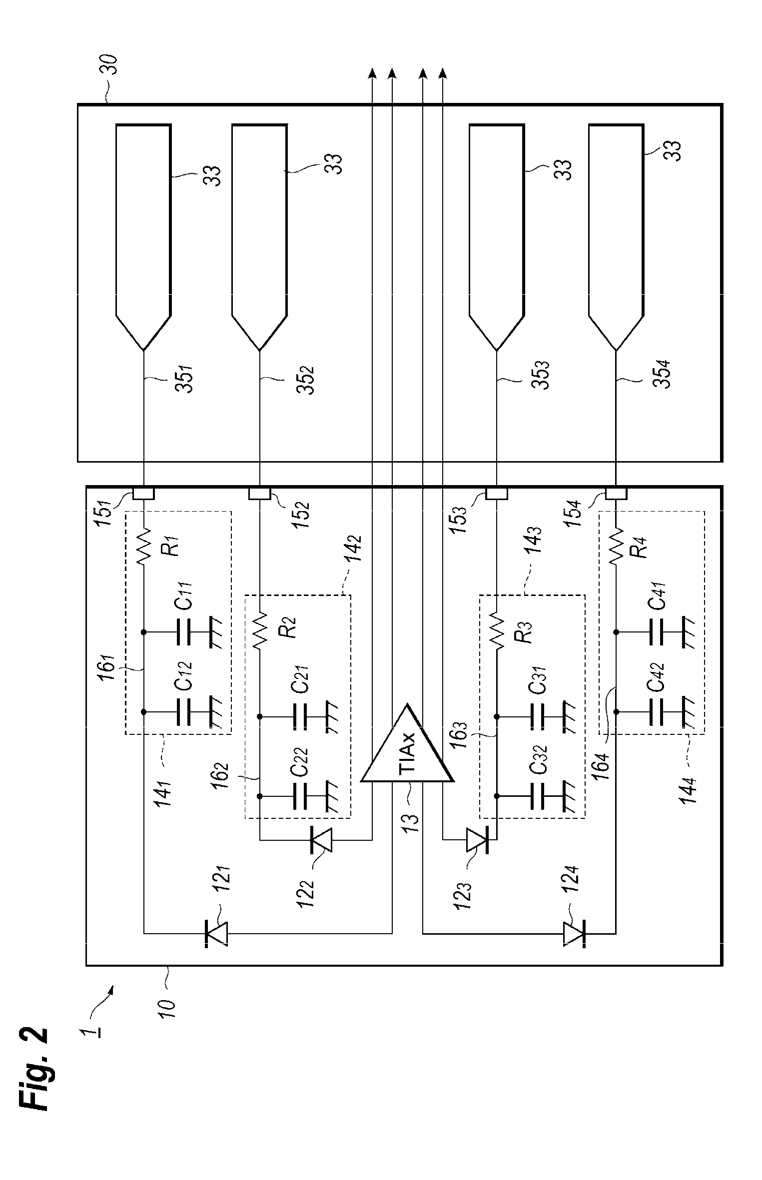
[0035]FIG. 4 shows a circuit diagram of an Rx module 10A and the PCB 30A according to the second embodiment of the present application. The Rx module 10A, and the PCB 30A of the second embodiment has a feature that the Rx module 10A provides, in addition to the first to fourth external bias lines 16n for the respective PDs 12n, a dummy unit 19 including an internal dummy line 17, a dummy terminal 18, and the PCB 30A provides an external dummy line 36 which is put between the signal lines 37 for the Tx module 20 and the first bias line 351 in the outside of the Rx module 10A. That is, the external dummy line 36 is arranged between the signal lines 37 for the Tx module 20 and the first external bias line disposed closest to the signal line 37. The first to fourth bias lines 35n are arranged closer to the signal line 37 in this order. Accordingly, the external dummy line 36 is most likely to be influence by the EMI noise due to the switching of large currents in the signal line 37, and...


PUM


Abstract

An optical transceiver that provides a receiver optical module including a plurality photodiodes (PDs) each biased through internal bias lines, signal lines carrying driving signals to an optical transmitter module, and external bias lines each connected to the internal bias lines. One of the internal bias lines connected to one of the external bias lines arranged closest to the signal lines has a length shorter than lengths of the other internal bias lines so as not to affect EMI noises induced from the signal lines to the other internal bias lines.

Description

BACKGROUND[0001]1. Field of the Invention[0002]The present application relates to an optical transceiver that transmits and receives wavelength multiplexed signals.[0003]2. Background Arts[0004]In order to eliminate noises superposed on power supply lines and / or bias lines, a technique to insert capacitors between the power supply lines, the bias lines and the ground has been well known in the circuit engineering. Many prior arts have disclosed such a technique.[0005]Recently, a new type of an optical transceiver becomes popular to solve a subject regarding to the communication capacity between servers. Such an optical transceiver has a transmission speed of exceeding 10 Gbps, sometimes reaching 40 Gbps and 100 Gbps and densely assembles many optical and electrical components therein. In such a high density assembly, the signal lines for an optical transmitter, which switch large currents, and the signal lines for an optical receiver, which carry signals with faint amplitude, are cl...

Claims


Application Information

Patent Timeline
Patent Type & Authority Applications(United States)
IPC IPC(8): H04B10/40H05K1/02H04J14/02H03H7/01
CPCH04B10/40H04J14/02H05K1/025H03H7/0138H03H1/02H04J14/0256H05K1/0218H05K2201/09781H01L2224/49171H01L2924/19107G02B6/428G02B6/4246G02B6/00
Inventor KASAI, SHINTANAKAJIMA, FUMIHIROONO, MASAAKI
Owner SUMITOMO ELECTRIC IND LTD
Why Eureka
Try Eureka