Electronic apparatus

a technology of electronic equipment and solder joints, applied in the direction of electrical equipment casings/cabinets/drawers, casings/cabinets/drawers details, electrical equipment contruction details, etc., can solve the problems of more dead space, inability to make electronic equipment smaller, so as to reduce the damage to the solder joint and mitigate the stress caused by the difference in thermal expansion coefficient between the solder joint and the board.

Inactive Publication Date: 2016-05-26
DENSO CORP
View PDF25 Cites 6 Cited by
  • Summary
  • Abstract
  • Description
  • Claims
  • Application Information

AI Technical Summary

Benefits of technology

[0015]As described above, the elastic deformable structure such that the board has the lower coefficient of elasticity in its thickness direction is provided in the portion where the through-hole is formed. Therefore, the stress caused by the difference in thermal expansion coefficient between the solder joint and the board can be mitigated

Problems solved by technology

However, according to a structure in that an external connection terminal is connected to the inside of a through-hole from an opposite surface to a surface on which a circuit constituting component is mounted, as in the structure disclosed in Patent Literature 1, there is created a dead space by the height of the housing, which makes it impossible to make the electronic apparatus smaller.
In particular, if a lead bending process is to be

Method used


Image

  • Electronic apparatus
  • Electronic apparatus
  • Electronic apparatus

Examples


first embodiment

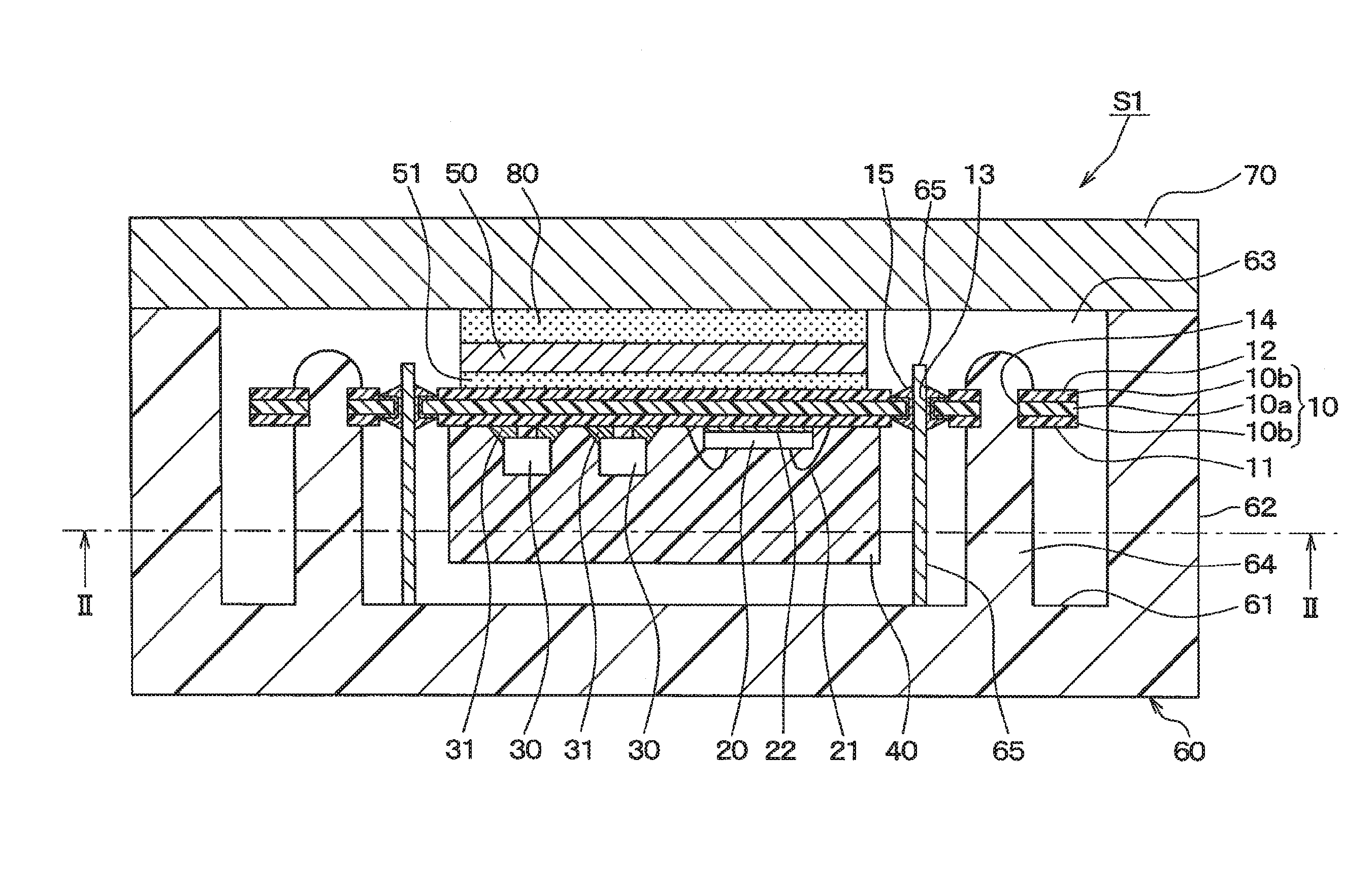
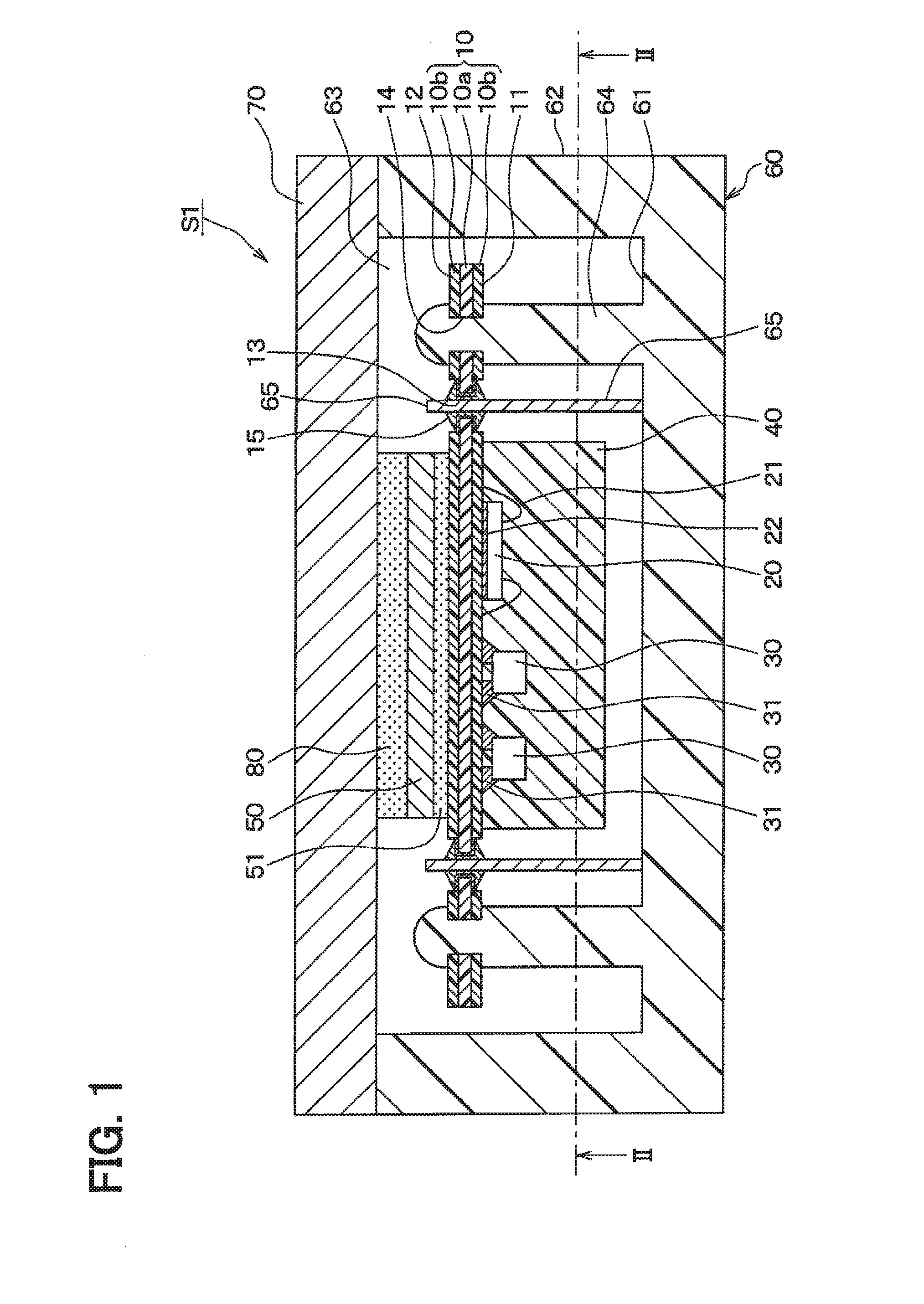
[0046]A general configuration of an electronic apparatus S1 according to a first embodiment of the present disclosure will be described with reference to FIGS. 1 to 3. The electronic apparatus S1 is mounted on a vehicle such as an automobile and is applied as an apparatus for driving various devices for the vehicle.

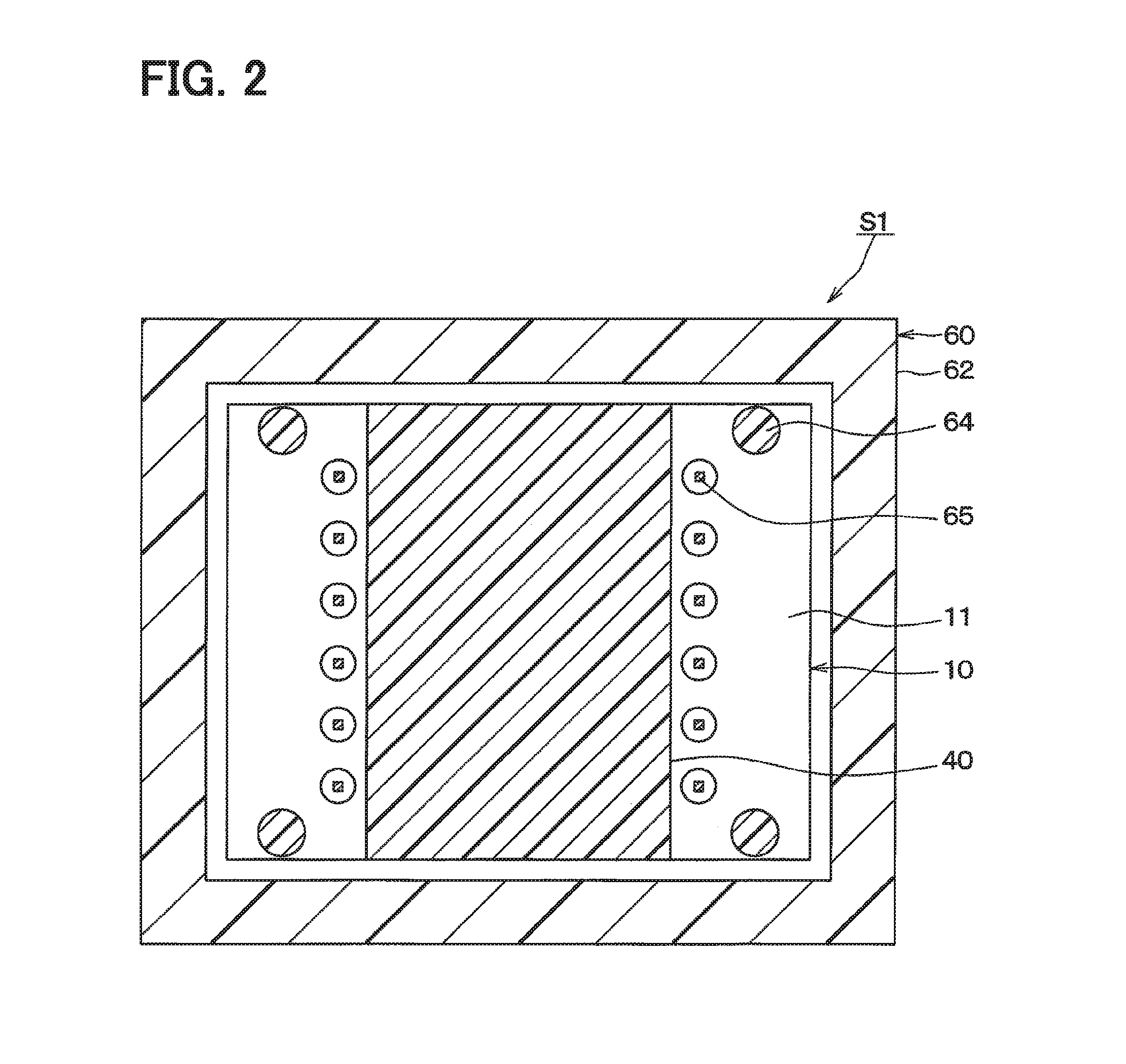
[0047]As shown in FIGS. 1 and 2, the electronic apparatus S1 is configured to include a board 10, electronic components 20 and 30, a mold resin 40, a heat sink 50, a case 60, a lid 70, a heat dissipating gel 80, and the like.

[0048]As shown in FIG. 1, the board 10 is formed of a plate-like member having a first surface 11 on which the electronic components 20 and 30 are mounted thereon and which is covered with the mold resin 40, and a second surface 12 opposite to the first surface 11. In this embodiment, the board 10 is formed as a plate-like member having a rectangular top plan shape as shown in FIG. 2, and is formed as a wiring board basically made of a resin such as a...

second embodiment

[0072]A second embodiment of the present disclosure will be described. This embodiment has a structure with reduced displacement in the through-holes 13 modified from that of the first embodiment. Since other features are the same as those of the first embodiment, parts that are different from the first embodiment only will be described.

[0073]As shown in FIG. 4, in this embodiment, the through-holes 13 are provided with a stress-relaxation member 10c made of a material having a lower thermal expansion coefficient than those of the constituent materials for the core layer 10a and buildup layers 10b inside the openings that form the through-holes 13 in the core layer 10a and buildup layers 10b. The openings in the core layer 10a and the buildup layers 10b have the equal size. The stress-relaxation member 10c is formed to cover the surfaces of the openings while leaving an opening for the connection terminal 65 to pass through. The through-holes 13 are configured by metal-plating the s...

third embodiment

[0076]A third embodiment of the present disclosure will be described. This embodiment has a structure with reduced displacement in through-holes 13 modified from that of the first embodiment. Since other features are the same as those of the first embodiment, parts that are different from the first embodiment only will be described.

[0077]As shown in FIG. 5, in this embodiment, in the portion where the through-holes 13 are formed, the size of the opening in the core layer 10a is made larger than the size of the openings in the buildup layers 10b. The stress-relaxation member 10c made of a material having a lower thermal expansion coefficient than that of the constituent material for the core layer 10a is provided inside the opening in the core layer 10a, similarly to the second embodiment. The through-holes 13 are configured by metal-plating the inner walls of the stress-relaxation member 10c and the buildup layers 10b, and the open ends of the buildup layers 10b.

[0078]As described ...


PUM


Abstract

An electronic apparatus includes a board, an electronic component, a mold resin a rod-like connection terminal and a case. The board includes: a first surface; a second surface, which is opposite to the first surface; a wire pattern; and a through-hole having a metal member connected to the wire pattern. The electronic component mounted on the first surface of the board. The mold resin seals the electronic component on the first surface of the board. The rod-like connection terminal inserted into the through-hole from a distal end of the through-hole and electrically connected to the metal member. The case having a surface on which the connection terminal stands and accommodating the board on which the electronic component is mounted. The board is arranged such that the first surface on which the electronic component and the mold resin are arranged faces the surface of the case on which the connection terminal stands.

Description

CROSS REFERENCE TO RELATED APPLICATION[0001]This application is based on Japanese Patent Application No. 2013-127549 filed on Jun. 18, 2013 and Japanese Patent Application No. 2014-106198 filed on May 22, 2014, the disclosure of which are incorporated herein by reference.TECHNICAL FIELD[0002]The present disclosure relates to an electronic apparatus having a structure in that a connection terminal is inserted into a through-hole in a board on which an electronic component is mounted, and is electrically connected to a wiring pattern formed on the board via a solder joint in the through-hole.BACKGROUND ART[0003]An electronic apparatus has hitherto been proposed, in Patent Literature 1, which has a structure in that a resin board with a circuit constituting component mounted thereon is encapsulated in a housing made of a mold resin, and an external connection terminal is connected to the inside of a through-hole formed in the resin board from an opposite side to the housing. Electrical...

Claims


Application Information

Patent Timeline
IPC IPC(8): H05K5/00H05K7/20H05K5/02H05K1/02H05K1/11
CPCH05K5/0004H05K1/0204H05K7/20409H05K5/0247H05K1/115H05K5/0056H05K1/0209H05K1/0271H05K1/116H05K3/284H05K3/3447H05K2201/066H01L2924/181H01L2224/48091H01L2924/13055H01L2924/13091H01L2924/00012H01L2924/00014H01L2924/00
Inventor TAKENAKA, MASAYUKIIMAIZUMI, NORIHISANAKAMURA, TOSHIHIRO
Owner DENSO CORP
Why Eureka
Try Eureka