Semiconductor module and power converter

Active Publication Date: 2016-06-02
MITSUBISHI ELECTRIC CORP
View PDF5 Cites 176 Cited by
  • Summary
  • Abstract
  • Description
  • Claims
  • Application Information

AI Technical Summary

Benefits of technology

The present invention aims to provide a semiconductor module that effectively shields magnetic fields generated by a semiconductor component. This invention is particularly useful for power converters that utilize the semiconductor module. The technical effect is to reduce interference between components in the semiconductor module, leading to improved performance and reliability.

Problems solved by technology

This magnetic field have adverse effects on operations of devices around the semiconductor component, and therefore should be shielded.
However, there has been a problem that the technique disclosed in Patent Document 1 cannot sufficiently shield the magnetic field.

Method used


Image

  • Semiconductor module and power converter
  • Semiconductor module and power converter
  • Semiconductor module and power converter

Examples


first embodiment

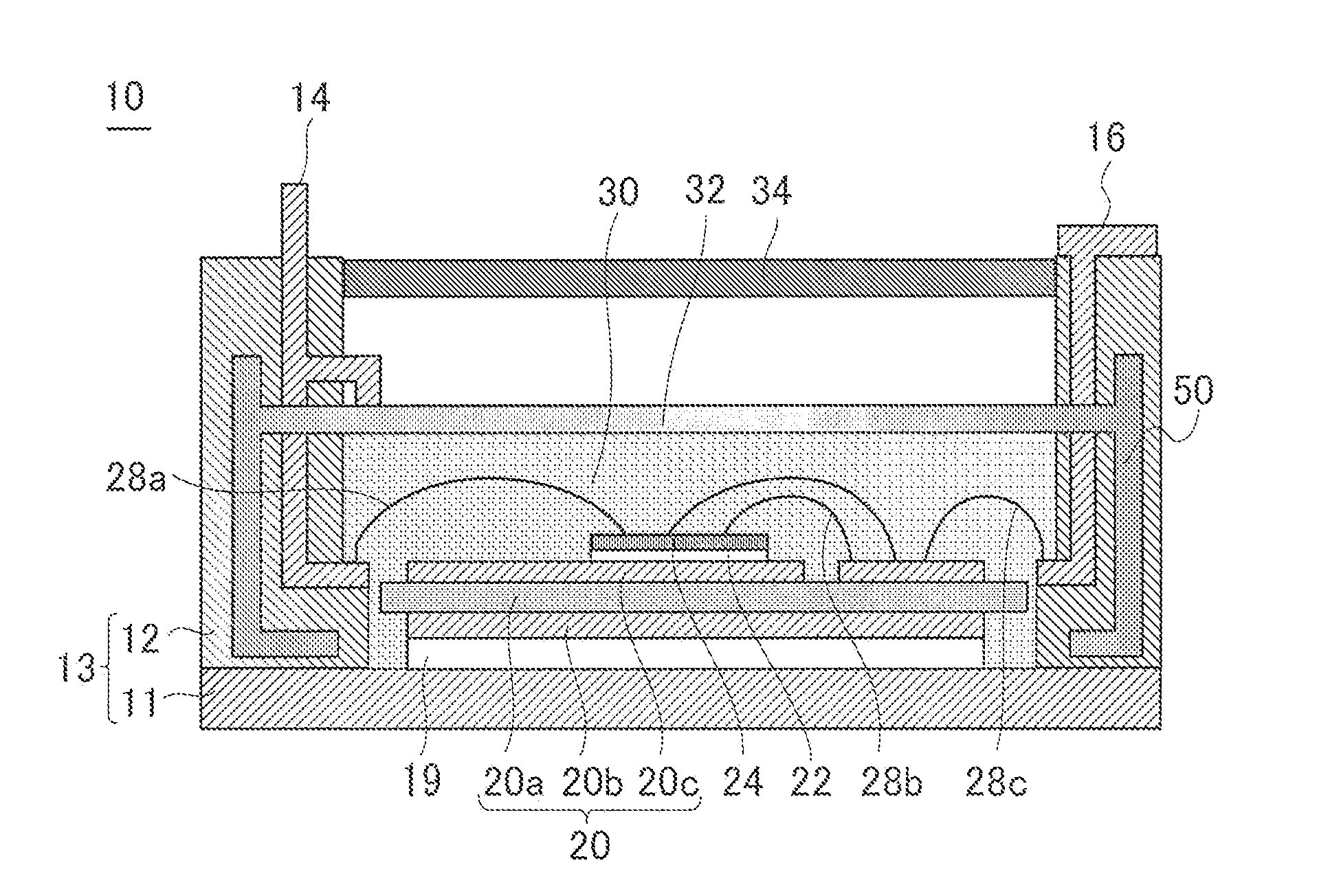
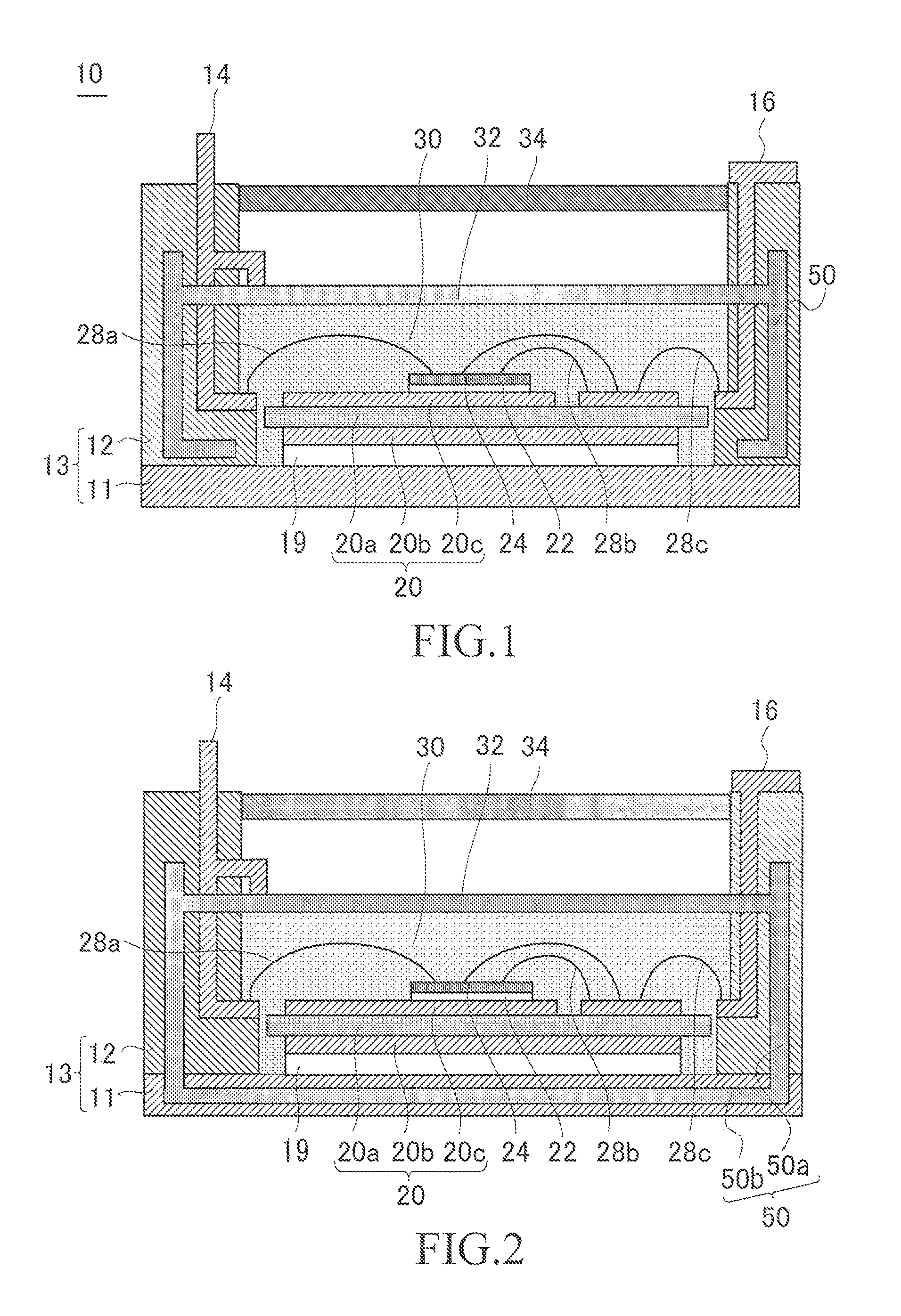
[0019]FIG. 1 is a cross-sectional view of a semiconductor module 10 according to first embodiment of the present invention. The semiconductor module 10 includes a case 13 including a base plate 11 and a wall portion 12. A signal terminal 14 and a power terminal 16 are embedded in the case 13. The signal terminal 14 includes a portion exposed to the inside of the case 13 and a portion exposed to the outside of the case 13. The power terminal 16 is configured similarly.

[0020]An insulating board 20 is fixed to the base plate 11 with solder 19. The insulating board 20 includes a ceramic substrate 20a, a metal layer 20b formed on a lower surface of the ceramic substrate 20a, and a metal pattern 20c formed on an upper surface of the ceramic substrate 20a.

[0021]A semiconductor component 24 is fixed to the metal pattern 20c with solder 22. The semiconductor component 24 is a component which switches a current, such as an IGBT (Insulated Gate Bipolar Transistor). In addition to the semicondu...

second embodiment

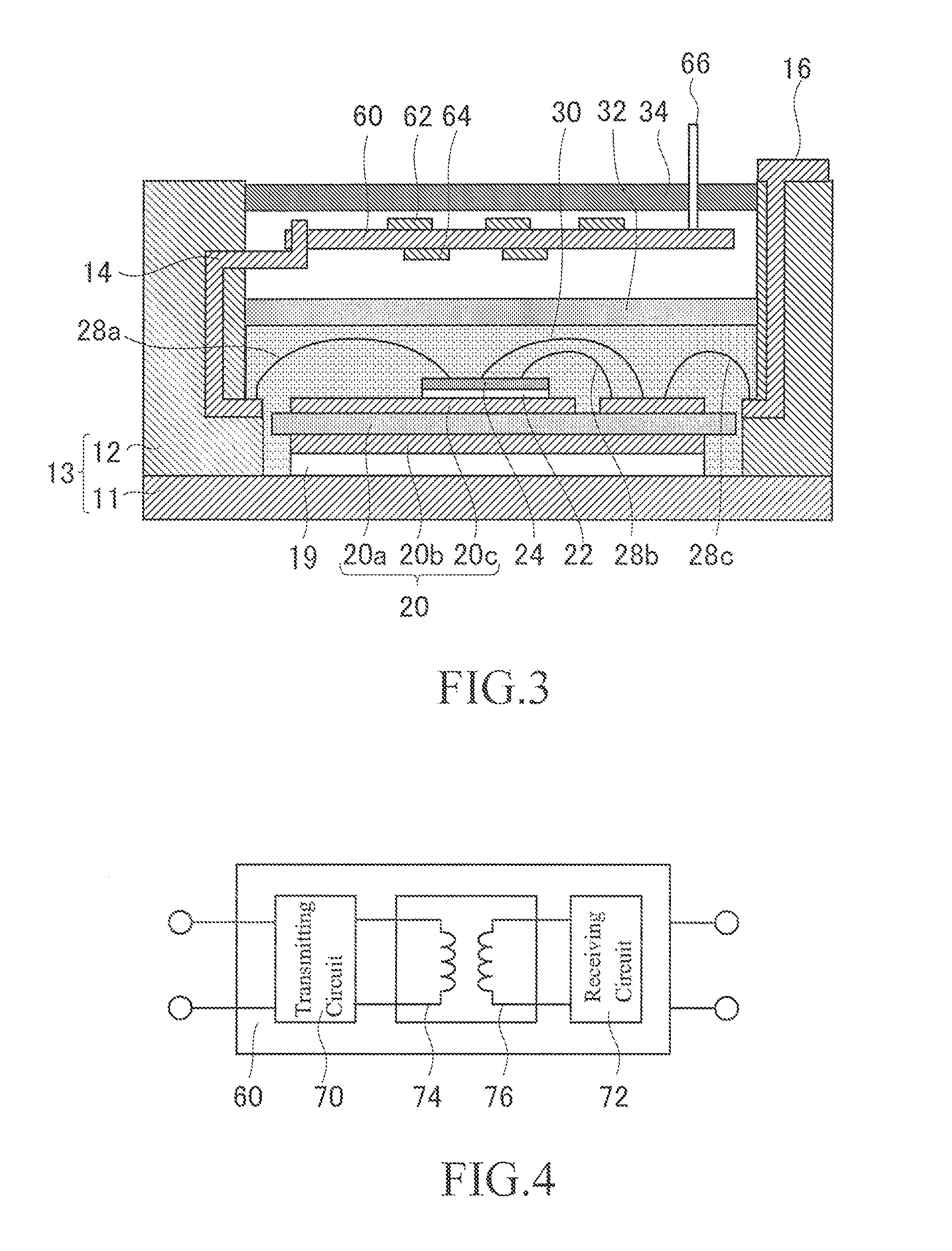
[0034]FIG. 3 is a cross-sectional view of a semiconductor module according to second embodiment. A control circuit board 60 is provided above the magnetic shield 32 in the case 13. The control circuit board 60 is, for example, a printed circuit board. Electronic components 62 and 64 are fixed to an upper surface and a lower surface of the control circuit board 60, respectively. A terminal 66 extending to the outside of the semiconductor module is fixed to the control circuit board 60. A control signal transmitted from the terminal 66 to the control circuit board 60 is subjected to a predetermined process in the electronic components 62 and 64 to reach the semiconductor component 24 through the signal terminal 14 and the wire 28a.

[0035]FIG. 4 is a view showing part of a circuit formed by electronic components fixed to the control circuit board 60. FIG. 4 shows a micro transformer structure. A micro transformer structure is configured such that two insulated coils 74 and 76 give and ...

third embodiment

[0037]FIG. 5 is a cross-sectional view of a semiconductor module according to third embodiment. A material having a higher thermal conductivity than the encapsulating resin 30 is mixed in the magnetic shield 32. This makes the thermal conductivity of the magnetic shield 32 higher than the thermal conductivity of the encapsulating resin 30. For example, since the thermal conductivity of the encapsulating resin 30 made of epoxy resin is 0.21 [W□m−1□K-311], a material having a thermal conductivity higher than the thermal conductivity thereof is mixed in the magnetic shield 32. In the case where a magnetic material contained in the magnetic shield 32 is ferrite powder, the ferrite powder often corresponds to the “material having a higher thermal conductivity than the encapsulating resin.” To sufficiently increase the thermal conductivity of the magnetic shield 32, a material having a very high thermal conductivity, such as gold, silver, or copper, is preferably mixed in the magnetic shi...


PUM


Abstract

A semiconductor module includes a case, a semiconductor component provided in the case for switching a current, encapsulating resin provided in the case for covering the semiconductor component, a magnetic shield contacting the encapsulating resin and containing a magnetic material, and an embedded magnetic shield embedded in the case, the embedded magnetic shield containing a magnetic material.

Description

BACKGROUND OF THE INVENTION[0001]1. Field of the Invention[0002]The present invention relates to a semiconductor module to be used for switching, for example, a large current, and a power converter including the semiconductor module.[0003]2. Background Art[0004]Japanese Patent Laid-Open No. H7-307416 discloses a semiconductor device in which conductive resin is provided on insulating resin covering a semiconductor component.[0005]When the semiconductor component performs switching, a magnetic field is generated around the semiconductor component. This magnetic field have adverse effects on operations of devices around the semiconductor component, and therefore should be shielded. However, there has been a problem that the technique disclosed in Patent Document 1 cannot sufficiently shield the magnetic field.SUMMARY OF THE INVENTION[0006]The present invention has been made to solve the above-described problem, and an object of the present invention is to provide a semiconductor modul...

Claims


Application Information

Patent Timeline
IPC IPC(8): H01L23/552H01L23/31
CPCH01L23/3114H01L23/552H01L24/29H01L24/32H01L24/48H01L24/49H01L24/73H01L25/072H01L2224/04026H01L2224/04042H01L2224/06181H01L2224/291H01L2224/32225H01L2224/48091H01L2224/48227H01L2224/48247H01L2224/49052H01L2224/73265H01L2924/10253H01L2924/10272H01L2924/1033H01L2924/13055H01L2924/19107H01L23/053H01L23/24H01L2924/00014H01L2924/181H01L2924/00012H01L2924/014H01L2224/45099H01L2224/45015H01L2924/207H01L2924/00
Inventor YONEYAMA, REIGOTO, AKIRA
Owner MITSUBISHI ELECTRIC CORP
Why Eureka
Try Eureka