2-terminal metal halide semiconductor/c-silicon multijunction solar cell with tunnel junction

Active Publication Date: 2016-06-09
THE BOARD OF TRUSTEES OF THE LELAND STANFORD JUNIOR UNIV +1
View PDF14 Cites 41 Cited by
  • Summary
  • Abstract
  • Description
  • Claims
  • Application Information

AI Technical Summary

Benefits of technology

[0008]The present invention provides a 2-terminal,MJ solar cell that avoids some of the disadvantages of the prior art. In some embodiments, the 2-terminal MJ solar cell is a tandem (two p-n junctions) solar cell having a thin film of metal halide semiconductor as the top solar-c

Problems solved by technology

However, very few materials exhibit high open-ci

Method used


Image

  • 2-terminal metal halide semiconductor/c-silicon multijunction solar cell with tunnel junction
  • 2-terminal metal halide semiconductor/c-silicon multijunction solar cell with tunnel junction
  • 2-terminal metal halide semiconductor/c-silicon multijunction solar cell with tunnel junction

Examples


Embodiment Construction

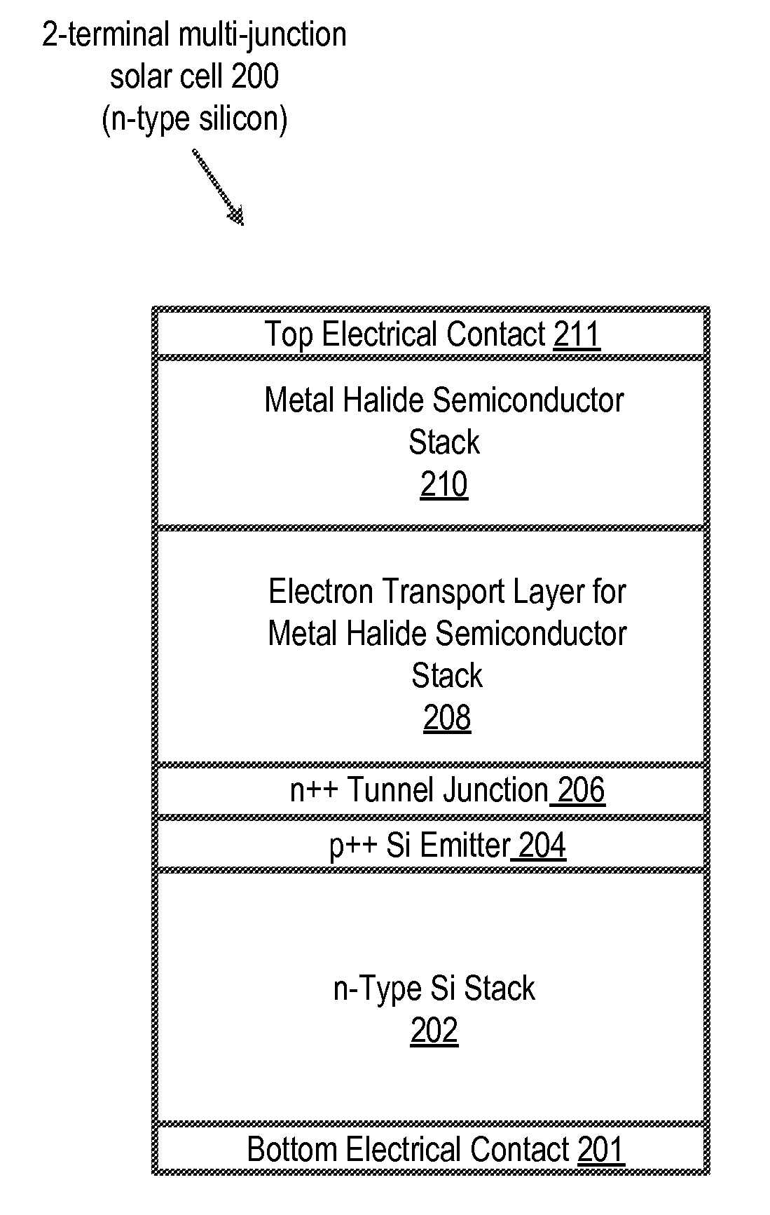
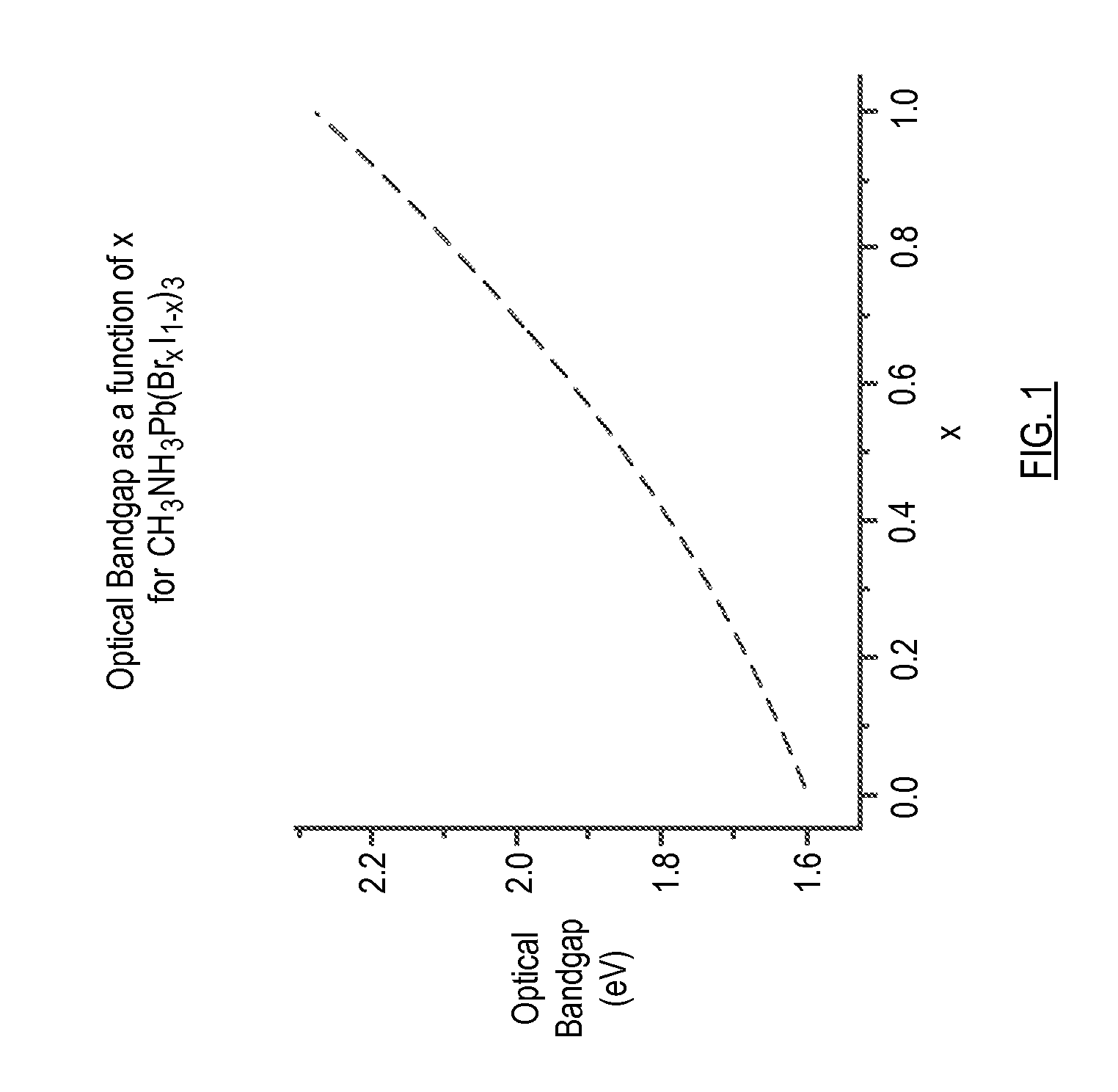
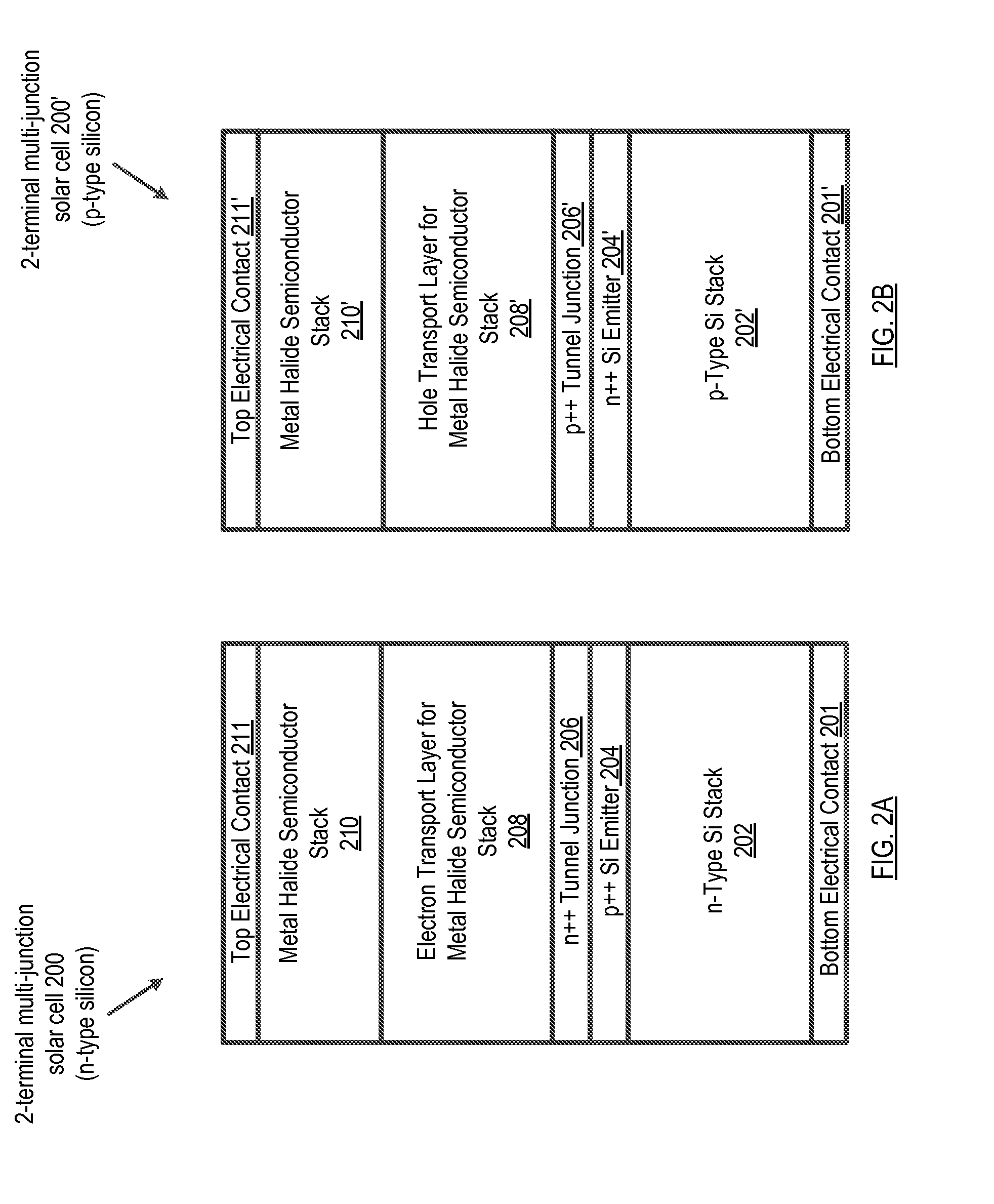
[0044]Definitions. A definition for each of the terms listed below is provided for use in understanding the description and interpreting the appended claims.[0045]“About” when referencing a measurement (e.g., diameter, length, thickness, etc.) means within 15% of the stated value.[0046]“Crystalline silicon” means monocrystalline, multi-crystalline, or polycrystalline.[0047]“Tandem” solar cell means a solar cell having two different absorbers (e.g., silicon and a metal halide semiconductor).[0048]“Multi-junction” solar cell means a solar cell having two or more absorbers (p-n junctions) in the same solar cell.[0049]“Nanowire” means electrically conductive material that is less than 1000 nanometers in diameter and greater than 1000 nanometers in length.[0050]“2-terminal” solar cell refers to a tandem solar cell in which the two sub-cells (e.g., the perovskite sub-cell and the silicon sub-cell) are electrically connected in series with each other. This is distinguished, for example, fr...


PUM


Abstract

A 2-terminal multi-junction solar cell having a thin film of metal halide semiconductor as the top solar-cell material and crystalline silicon as the bottom solar-cell material. In the illustrative embodiment, the top solar-cell material is a perovskite of the form AM(IxH1-x)3, where A is a cation, preferably methylammonium (CH3NH3), formamidinium ([R2N—CH═NR2]+), or cesium; M is metal, preferably Pb, Sn, Ge; H is a halide, preferably Br or Cl; and x=iodine fraction, in the range of 0 to 1, inclusive. The integration of the two solar-cell materials is enabled by the use of a tunnel junction composed of indirect band-gap material.

Description

STATEMENT REGARDING FEDERALLY SPONSORED RESEARCH[0001]This case claims priority to U.S. patent application 62 / 086785 filed Dec. 3, 2014 and which is incorporated herein by reference.STATEMEMT REGARDING FEDERALLY SPONSORED RESEARCH[0002]This invention was made with Government support under Grant Nos. DE-EE0004946 and DE-EE0006707 awarded by the U.S. Department of Enegry. The Government has certain rights in the invention.FIELD OF THE INVENTION[0003]The present invention relates generally to solar cells.BACKGROUND OF THE INVENTION[0004]Solar-to-electricity conversion efficiency is the key technical driver influencing photovoltaic (PV) module costs. The record efficiency of crystalline silicon (c-Si) single-junction PV devices increased from 25% to 25.6% during the last fifteen years, asymptotically approaching the Shockley-Queisser (S-Q) efficiency limit of 29.4%. To exceed this efficiency limit, multi-junction solar cells have been proposed.[0005]Multi-junction (MJ) solar cells have ...

Claims


Application Information

Patent Timeline
IPC IPC(8): H01L31/078H01L31/0725H01L31/18H01L31/0224H01L51/42H01L31/02H01L31/0336
CPCH01L31/078H01L31/02008H01L31/0725H01L31/18H01L31/022425H01L51/4213H01L31/0336H01L31/043Y02E10/549H10K30/57H10K85/00H10K30/151H10K85/50H10K30/10
Inventor MAILOA, JONATHAN P.BAILIE, COLIN DAVIDJOHLIN, ERIC CARLMCGEHEE, MICHAEL DAVIDBUONASSISI, TONIO
Owner THE BOARD OF TRUSTEES OF THE LELAND STANFORD JUNIOR UNIV
Why Eureka
Try Eureka