Microvia structure of flexible circuit board and manufacturing method thereof

a flexible circuit board and microvia technology, applied in the field of microvia structure can solve the problems of no longer satisfying the needs of modern industries, adverse to the use of flexible circuit boards, etc., and achieve the effects of reducing circuit impedance, ensuring conduction reliability, and extending conductive contact surface area

Active Publication Date: 2016-06-23
ADVANCED FLEXIBLE CIRCUITS
View PDF2 Cites 3 Cited by
  • Summary
  • Abstract
  • Description
  • Claims
  • Application Information

AI Technical Summary

Benefits of technology

[0016]In the efficacy, compared to the prior art, the present involve a simple process that allows for formation of a microvia structure in a flexible circuit board without application of electroplating. Further, in the present invention, the conductive paste layer is filled in the second through hole of the second conductive layer, the dielectric layer through hole of the dielectric layer, and the first through hole of the first conductive layer in such a way that the conductive paste layer effectively covers and contacts the first exposed zone of the first conductive layer and the second exposed zone of the second conductive laye...

Problems solved by technology

The conventional via structure of the flexible circuit board, although fit to the uses of the electronic circuits, no longer satisfies the need of the modern industries when the conductive traces and spacing distances therebetween get smal...

Method used


Image

  • Microvia structure of flexible circuit board and manufacturing method thereof
  • Microvia structure of flexible circuit board and manufacturing method thereof
  • Microvia structure of flexible circuit board and manufacturing method thereof

Examples


Embodiment Construction

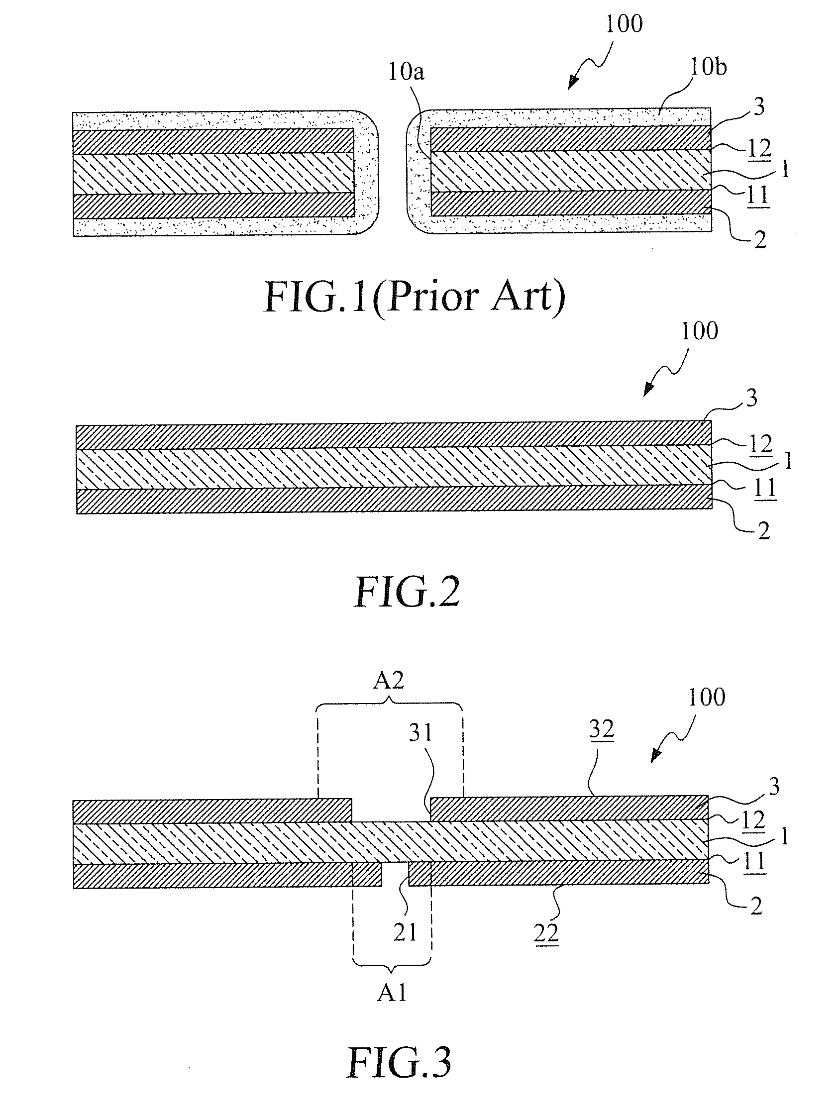
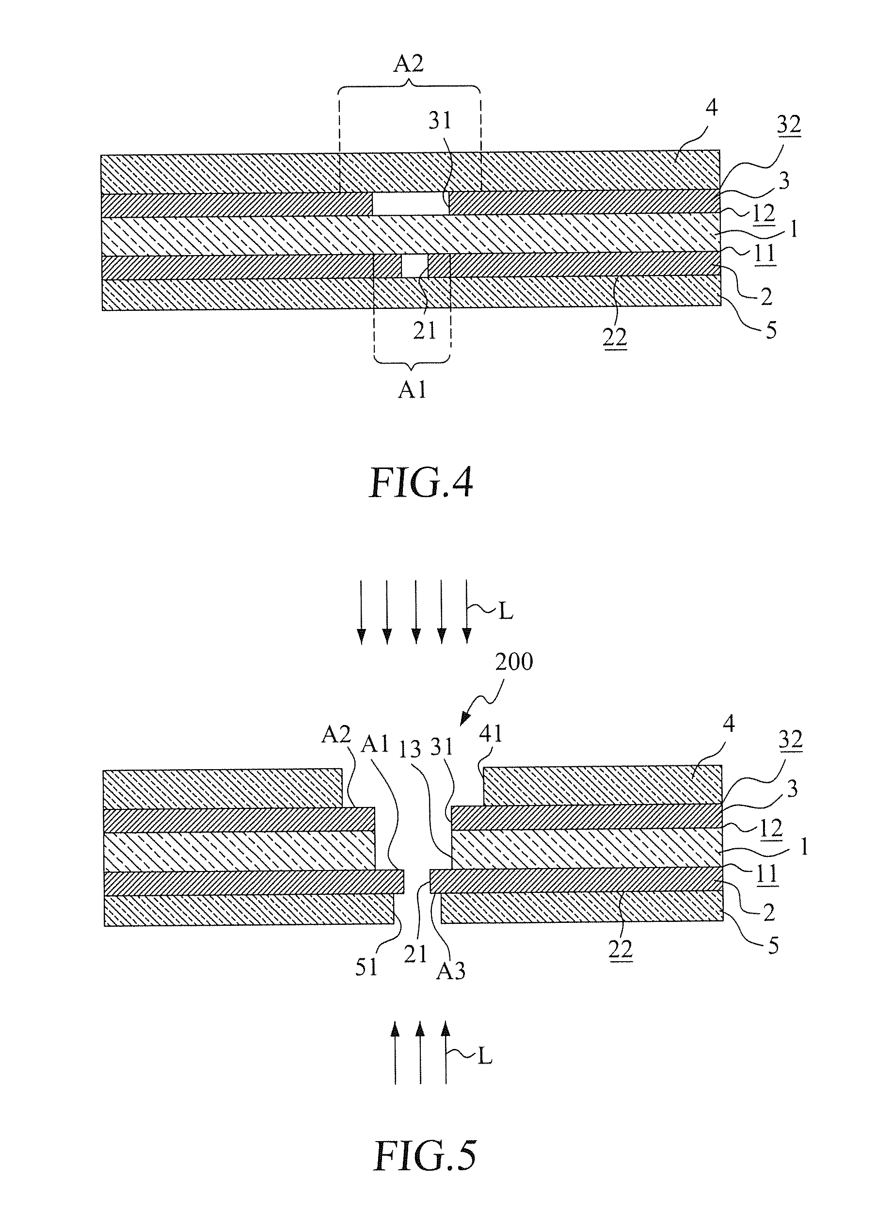
[0035]Referring to FIGS. 2-8, schematic views, in a sectioned form, are given to illustrate the manufacture of a microvia structure of a flexible circuit board according to a first embodiment of the present invention. FIG. 9 is a flow chart illustrating the process of the first embodiment of the present invention. The structure and the manufacturing method of the first embodiment of the present invention will be described with reference to FIGS. 2-9.

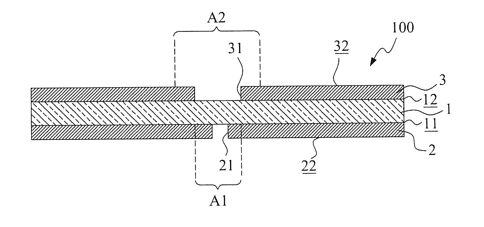
[0036]As shown in FIG. 2, in the manufacture of the microvia structure of the flexible circuit board according to the present invention, a flexible circuit board 100 (Step 101) is first prepared. The flexible circuit board 100 comprises a dielectric layer 1, a first conductive layer 2, and a second conductive layer 3, in which the first conductive layer 2 and the second conductive layer 3 are respectively formed on a first surface 11 and a second surface 12 of the dielectric layer 1.

[0037]As shown in FIG. 3, a first through hole 21 is fo...


PUM


Abstract

Disclosed urea microvia structure of a flexible circuit board and a manufacturing method thereof. A first through hole is formed in a first conductive layer of a flexible circuit board and a first exposed zone is defined. A second conductive layer includes a second through hole formed therein and defines a second exposed zone. A dielectric layer includes a dielectric layer through hole corresponding to the second through hole of the second conductive layer. A conductive paste layer is filled in the second through hole of the second conductive layer, the dielectric layer through hole of the dielectric layer, and the first through hole of the first conductive layer in such a way that the conductive paste layer covers and electrically contacts the first exposed zone of the first conductive layer and the second exposed zone of the second conductive layer.

Description

BACKGROUND OF THE INVENTION[0001]1. Field of the Invention[0002]The present invention relates to a flexible circuit board microvia technology and in particular to a microvia structure of a flexible circuit board and a manufacturing method thereof, which provide advantages of enlarged conductive contact surface area, reduced impedance, and ensured conduction reliability.[0003]2. The Related Arts[0004]The flexible circuit technology has been widely used in all sorts of electronic equipment, communication equipment, and instruments. To achieve a desired circuit arrangement, it is common to form conductive traces and via structures on and in a flexible circuit board. FIG. 1 is a schematic view that illustrates a conventional via structure formed in a flexible circuit board. The flexible circuit board has a structure that comprises a dielectric layer, a first conductive layer, and a second conductive layer, in which the first conductive layer and the second conductive layer are respectiv...

Claims


Application Information

Patent Timeline
IPC IPC(8): H05K1/11H05K3/40H05K3/06H05K1/09
CPCH05K1/115H05K3/06H05K3/4038H05K1/092H05K1/0251H05K3/4069H05K2201/0397H05K2201/09845H05K2201/09854
Inventor SU, KUO-FULIN, GWUN-JIN
Owner ADVANCED FLEXIBLE CIRCUITS
Why Eureka
Try Eureka