High conductance process kit

a technology of process kit and high conductance, which is applied in the direction of coating, chemical vapor deposition coating, electric discharge tube, etc., can solve the problems of affecting chip yield, parts making up the process kit need to be cleaned or replaced,

Active Publication Date: 2016-06-30
APPLIED MATERIALS INC
View PDF6 Cites 14 Cited by
  • Summary
  • Abstract
  • Description
  • Claims
  • Application Information

AI Technical Summary

Benefits of technology

[0009]In various instances, a process kit for a plasma processing chamber includes a gas diffuser configured to be arranged within a circular aperture on an upper shield for a plasma processing chamber. The gas diffuser includes a cylindrical housing t...

Problems solved by technology

However, some of the contaminant and/or etched material may be deposited on surfaces of the chamber.
Eventually, the parts making up the process kit need to be c...

Method used


Image

  • High conductance process kit
  • High conductance process kit
  • High conductance process kit

Examples


Embodiment Construction

[0026]Aspects of a process kit described herein can provide more efficient plasma processing while reducing the buildup of contaminants on surfaces of the process kit. Contaminants on surfaces of the process kit could become particle sources that could contaminate substrates in the chamber and affect chip yield.

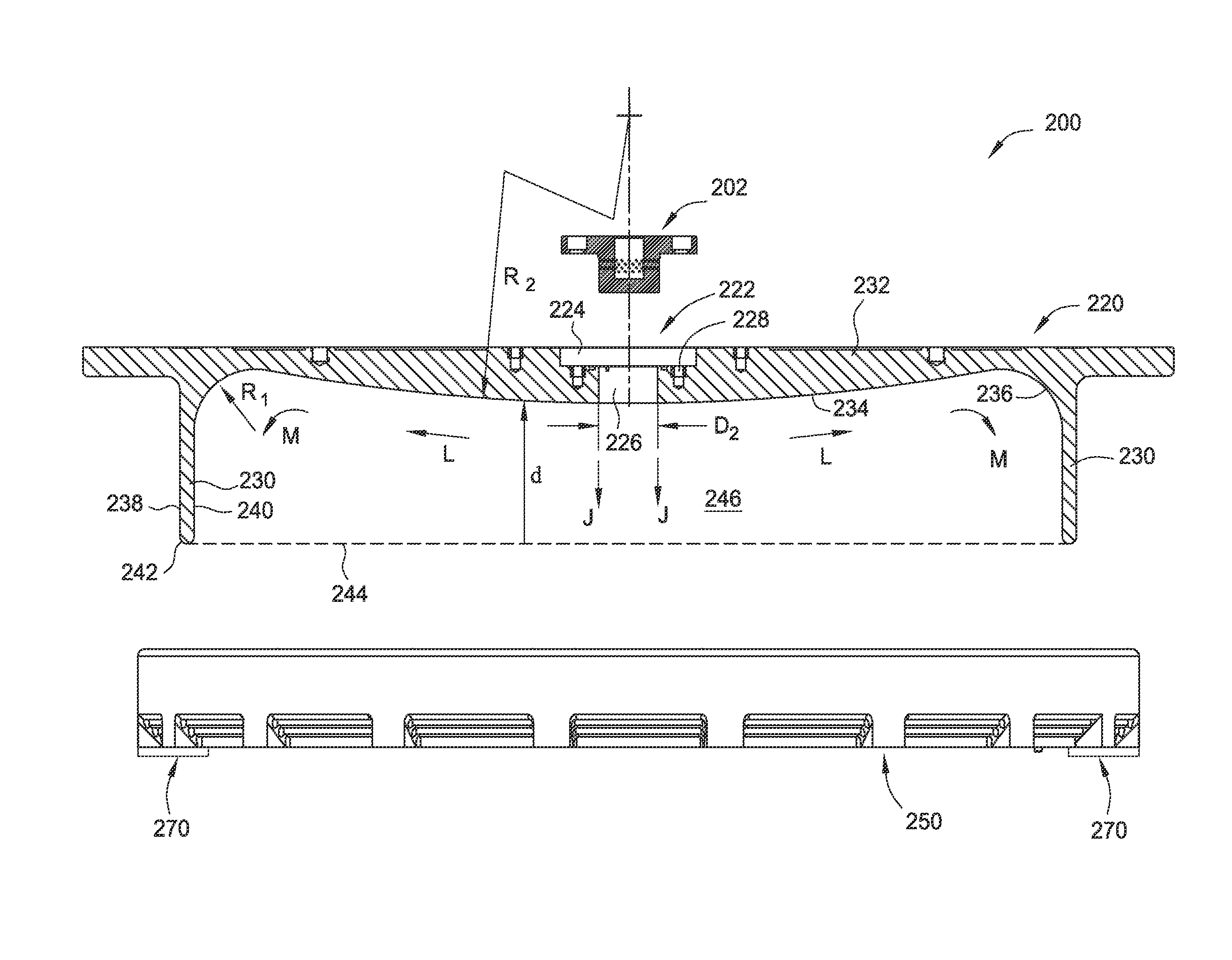
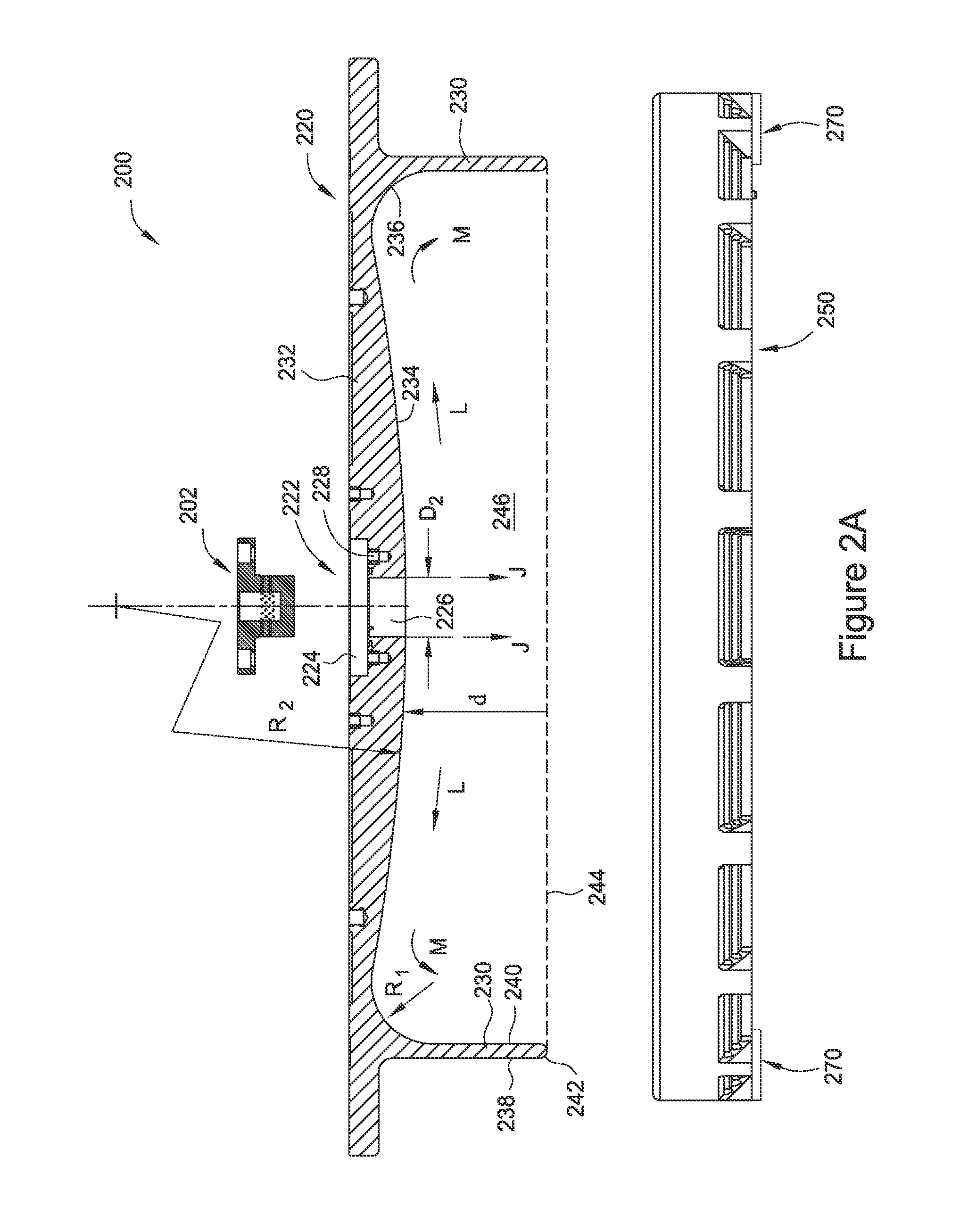
[0027]FIG. 2A is an exploded side view of a process kit 200 according to various aspects for use in a plasma processing chamber. FIG. 2B shows the process kit 200 arranged in a plasma processing chamber 300. The process kit 200 includes at least one or more of a diffuser 202, an upper shield 220, and a lower shield 250, 270. The diffuser 202 sits within an aperture 222 in the upper shield 220 such that process gas is injected through the diffuser 202 and the upper shield 220 in the middle or center of the upper shield 220 rather than along the perimeter of the upper shield 110 shown in FIG. 1. The upper shield 220 and the lower shield 250, 270 include rounded corners that hel...


PUM

PropertyMeasurementUnit
Diameteraaaaaaaaaa
Diameteraaaaaaaaaa
Radiusaaaaaaaaaa

Abstract

Apparatus for plasma processing of semiconductor substrates. Aspects of the apparatus include an upper shield with a gas diffuser arranged at a center of the upper shield. The gas diffuser and upper shield admit a process gas to a processing chamber in a laminar manner. A profile of the upper shield promotes radial expansion of the process gas and radial travel of materials etched from a surface of the substrates. Curvatures of the upper shield direct the etched materials to a lower shield with reduced depositing of etched materials on the upper shield. The lower shield also includes curved surfaces that direct the etched materials toward slots that enable the etched materials to exit from the process chamber with reduced depositing on the lower shield.

Description

BACKGROUND[0001]1. Field[0002]Embodiments of the present invention generally relate to plasma cleaning or etching in the process of fabricating integrated circuits. In particular, the invention relates to a process kit for a plasma chamber.[0003]2. Description of the Related Art[0004]Plasma chambers are used in integrated circuit manufacturing to remove contaminants from the surface of a substrate and / or to etch surfaces of a substrate. To perform a plasma cleaning or etching process, an integrated circuit is placed in a plasma chamber and a pump removes most of the air from the chamber. A gas, such as argon, can then be injected into the chamber. Electromagnetic energy (e.g., radio frequency) is applied to the injected gas to excite the gas into a plasma state. The plasma releases ions that bombard the surface of the substrate to remove contaminants and / or material from the substrate. Atoms or molecules of the contaminants and / or substrate material are etched from the substrate and...

Claims


Application Information

Patent Timeline
IPC IPC(8): H01J37/32H01L21/67
CPCH01J37/32651H01J37/3244H01J37/32642H01J2237/006H01J2237/0268H01J2237/334H01L21/67069H01J37/32477C23C16/45563C23C16/45565H01J2237/335
Inventor CHIA, BONNIE T.TSAI, CHENG-HSIUNG
Owner APPLIED MATERIALS INC
Why Eureka
Try Eureka