Semiconductor device and manufacturing method thereof

a semiconductor and semiconductor technology, applied in the direction of semiconductor devices, electrical equipment, transistors, etc., can solve the problems of low power consumption of display devices for which a transistor including an oxide semiconductor is used, and achieve the effects of low power consumption, high reliability, and low off-state curren

Inactive Publication Date: 2016-06-30
SEMICON ENERGY LAB CO LTD
View PDF6 Cites 3 Cited by
  • Summary
  • Abstract
  • Description
  • Claims
  • Application Information

AI Technical Summary

Benefits of technology

[0020]An object of one embodiment of the present invention is to provide a semiconductor device including a transistor with low off-state current. Another object of one embodiment of the present invention is to provide a semiconductor device with low power consumption. Another object of one embodiment of the present invention is to provide a miniaturized semiconductor device. Another object of one embodiment of the present invention is to provide a highly reliable semiconductor device. Another object of one embodiment of the present invention is to provide a semiconductor device capable of high-speed writing. Another object of one embodiment of the present invention is to provide a semiconductor device capable of high-speed reading. Another object of one embodiment of the present invention is to provide a semiconductor device capable of retaining data for a long period. Another object of one embodiment of the present invention is to provide a novel semiconductor device. Another object of one embodiment of the present invention is to provide an eye-friendly display device. Another object of one embodiment of the present invention is to provide a semiconductor device including a transparent semiconductor.
[0032]A semiconductor device or the like including a transistor with low off-state current can be provided. A semiconductor device with low power consumption can be provided. A miniaturized semiconductor device can be provided. A highly reliable semiconductor device can be provided. A semiconductor device capable of high-speed writing can be provided. A semiconductor device capable of retaining data for a long period can be provided. A semiconductor device capable of high-speed reading can be provided. A novel semiconductor device can be provided. An eye-friendly display device can be provided. A semiconductor device including a transparent semiconductor can be provided.

Problems solved by technology

For example, a display device for which a transistor including an oxide semiconductor is used is known to have low power consumption.

Method used


Image

  • Semiconductor device and manufacturing method thereof
  • Semiconductor device and manufacturing method thereof
  • Semiconductor device and manufacturing method thereof

Examples


embodiment 1

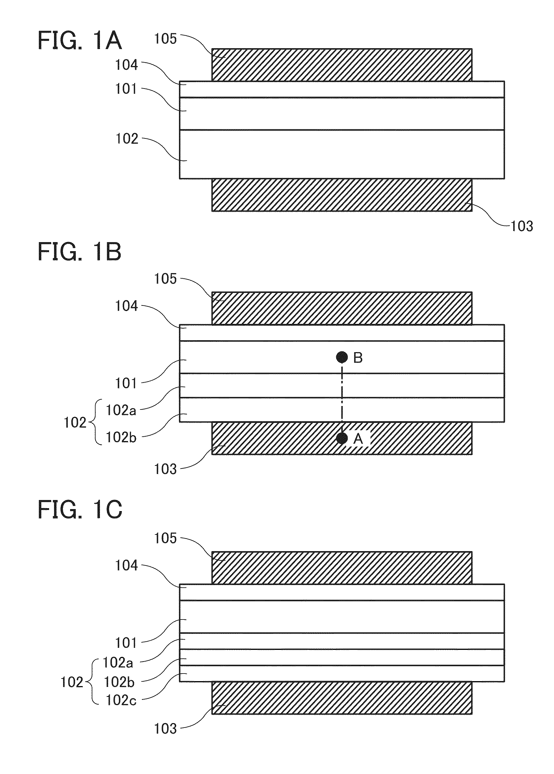
[0089]In this embodiment, a structure of a semiconductor device including a semiconductor, an electron trap layer, and a gate electrode, the operation principle of the semiconductor device, and a circuit that uses the semiconductor device are described. FIG. 1A shows a semiconductor device including a semiconductor 101, an electron trap layer 102, a gate electrode 103, a gate insulator 104, and a gate electrode 105.

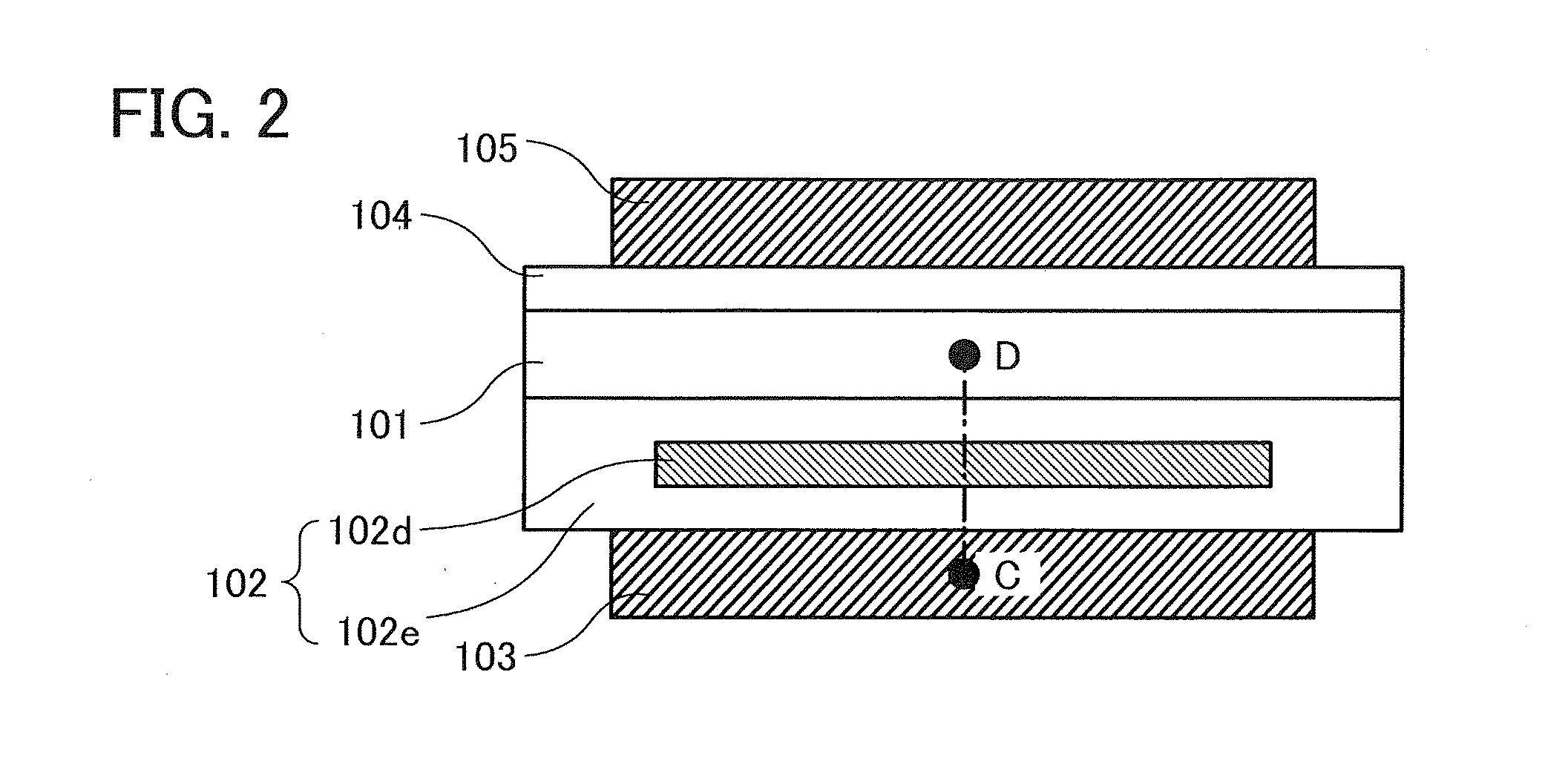
[0090]The electron trap layer 102 may be, for example, a stack including an insulator 102a and an insulator 102b as illustrated in FIG. 1B. Alternatively, the electron trap layer 102 may be a stack including the insulator 102a, the insulator 102b, and an insulator 102c as illustrated in FIG. 1C. Alternatively, the electron trap layer 102 may be a stack including more insulators. Alternatively, as illustrated in FIG. 2, the electron trap layer 102 may include an insulator 102e and an electrically isolated conductor 102d in the insulator 102e. The insulator 102e may be comp...

embodiment 2

[0129]In this embodiment, a structure of a transistor of one embodiment of the present invention is described with reference to drawings.

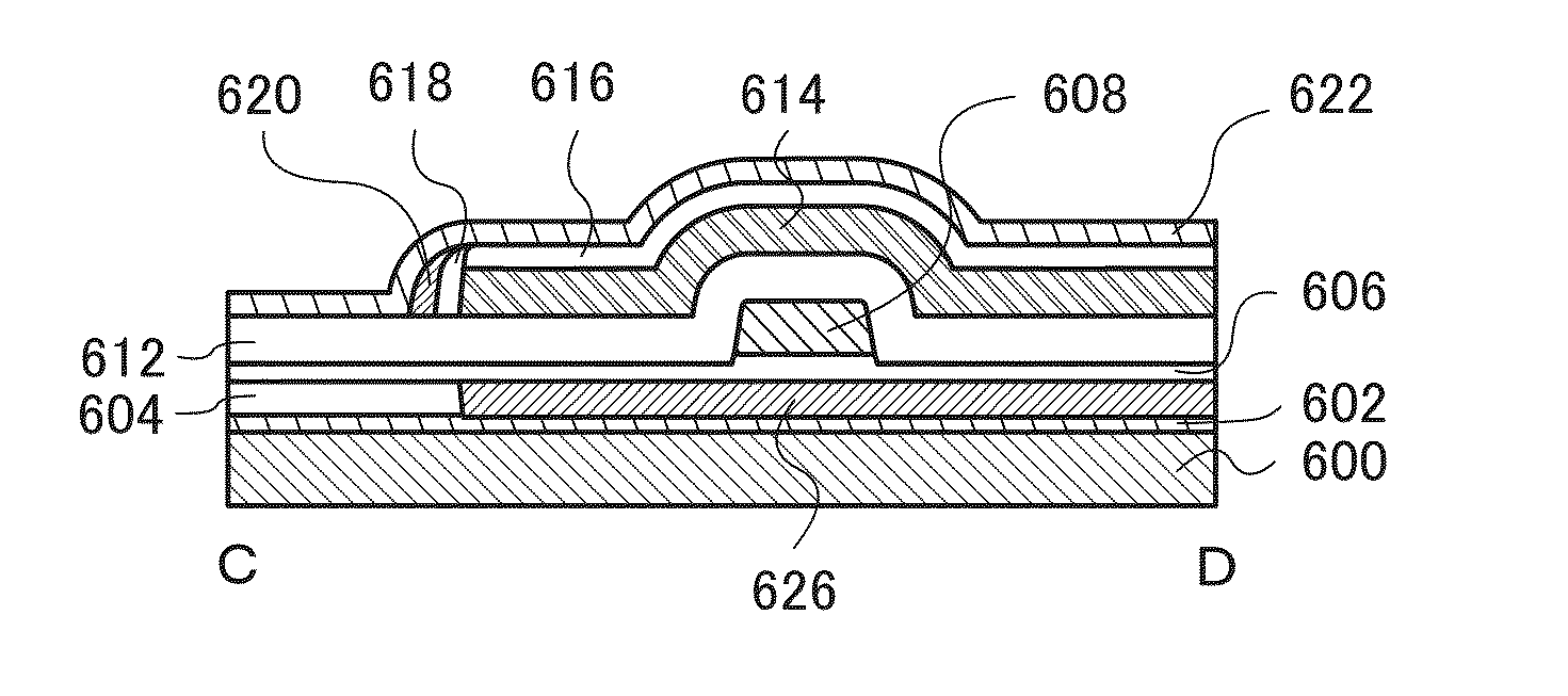
[0130]FIGS. 5A to 5C are a top view and cross-sectional views that illustrate a transistor of one embodiment of the present invention. FIG. 5A is the top view. FIG. 5B illustrates a cross section taken along the dashed-dotted line A-B in FIG. 5A. FIG. 5C illustrates a cross section taken along the dashed-dotted line C-D in FIG. 5A. Note that for simplification of the drawing, some components are not illustrated in the top view of FIG. 5A. In some cases, the direction of the dashed-dotted line A-B is referred to as a channel length direction, and the direction of the dashed-dotted line C-D is referred to as a channel width direction.

[0131]The transistor illustrated in FIGS. 5A to 5C includes an insulator 602 over a substrate 600, an insulator 604 over the insulator 602, an insulator 606 over the insulator 604, an oxide semiconductor 608 over the ins...

embodiment 3

[0183]In this embodiment, a method for controlling the threshold voltage of a transistor is described with reference to FIGS. 13A and 13B. FIG. 13A is circuit diagrams illustrating a transistor 120 and a transistor 140. A dotted line in the circuit diagram denotes an electron trap layer. FIG. 13B is cross-sectional schematic diagrams illustrating the transistor 120 and the transistor 140.

[0184]The transistor 120 and the transistor 140 are formed over a substrate 601. The transistor 120 includes an oxide semiconductor 609a, a source electrode 611a, a drain electrode 611b, a gate electrode 627a, and an electron trap layer 621a. The electron trap layer 621a includes a region overlapping with the oxide semiconductor 609a. The transistor 140 includes an oxide semiconductor 609b, a source electrode 611c, a drain electrode 611d, a gate electrode 627b, and an electron trap layer 621b. The electron trap layer 621b includes a region overlapping with the oxide semiconductor 609b. The transisto...


PUM


Abstract

To provide a semiconductor device suitable for high reliability and high-speed operation. The semiconductor device includes a first conductor, a first insulator, a second insulator, a semiconductor, and an electron trap layer. The semiconductor includes a channel formation region. The first conductor includes a region overlapping with the channel formation region with the first insulator provided therebetween. The second insulator is placed to include a region in contact with a side surface of the first conductor. The electron trap layer is placed to face the first conductor with the second insulator provided therebetween.

Description

BACKGROUND OF THE INVENTION[0001]1. Field of the Invention[0002]The present invention relates to an object, a method, or a manufacturing method. The present invention relates to a process, a machine, manufacture, or a composition of matter. One embodiment of the present invention relates to a semiconductor device, a display device, a light-emitting device, a power storage device, an imaging device, a memory device, a driving method thereof, or a manufacturing method thereof. In particular, one embodiment of the present invention relates to a semiconductor device, a display device, or a light-emitting device each including an oxide semiconductor.[0003]In this specification and the like, a semiconductor device generally means a device that can function by utilizing semiconductor characteristics. A display device, a light-emitting device, a lighting device, an electro-optical device, a semiconductor circuit, and an electronic device include a semiconductor device in some cases.[0004]2....

Claims


Application Information

Patent Timeline
Patent Type & Authority Applications(United States)
IPC IPC(8): H01L29/786H01L21/479H01L27/12
CPCH01L29/78606H01L29/7869H01L29/78696H01L21/479H01L27/1251H01L27/124H01L27/1259H01L27/1225H01L29/42384H01L29/66969H01L29/78603H01L29/78648H01L29/40117H01L29/66833H01L29/792H01L29/4234H01L29/7883
Inventor TANAKA, TETSUHIROMATSUBAYASHI, DAISUKETANEMURA, KAZUKI
Owner SEMICON ENERGY LAB CO LTD
Why Eureka
Try Eureka