
Generation of Flexible High Power Pulsed Waveforms

a high-power pulsed waveform and flexible technology, applied in the field of flexible, high-power pulsed waveform generation, can solve the problems of limited voltage holding capacity of silicon technology, and large malfunction of the receiving apparatus

Active Publication Date: 2016-07-07
BAE SYST INFORMATION & ELECTRONICS SYST INTERGRATION INC
View PDF26 Cites 4 Cited by
  • Summary
  • Abstract
  • Description
  • Claims
  • Application Information

AI Technical Summary

Benefits of technology

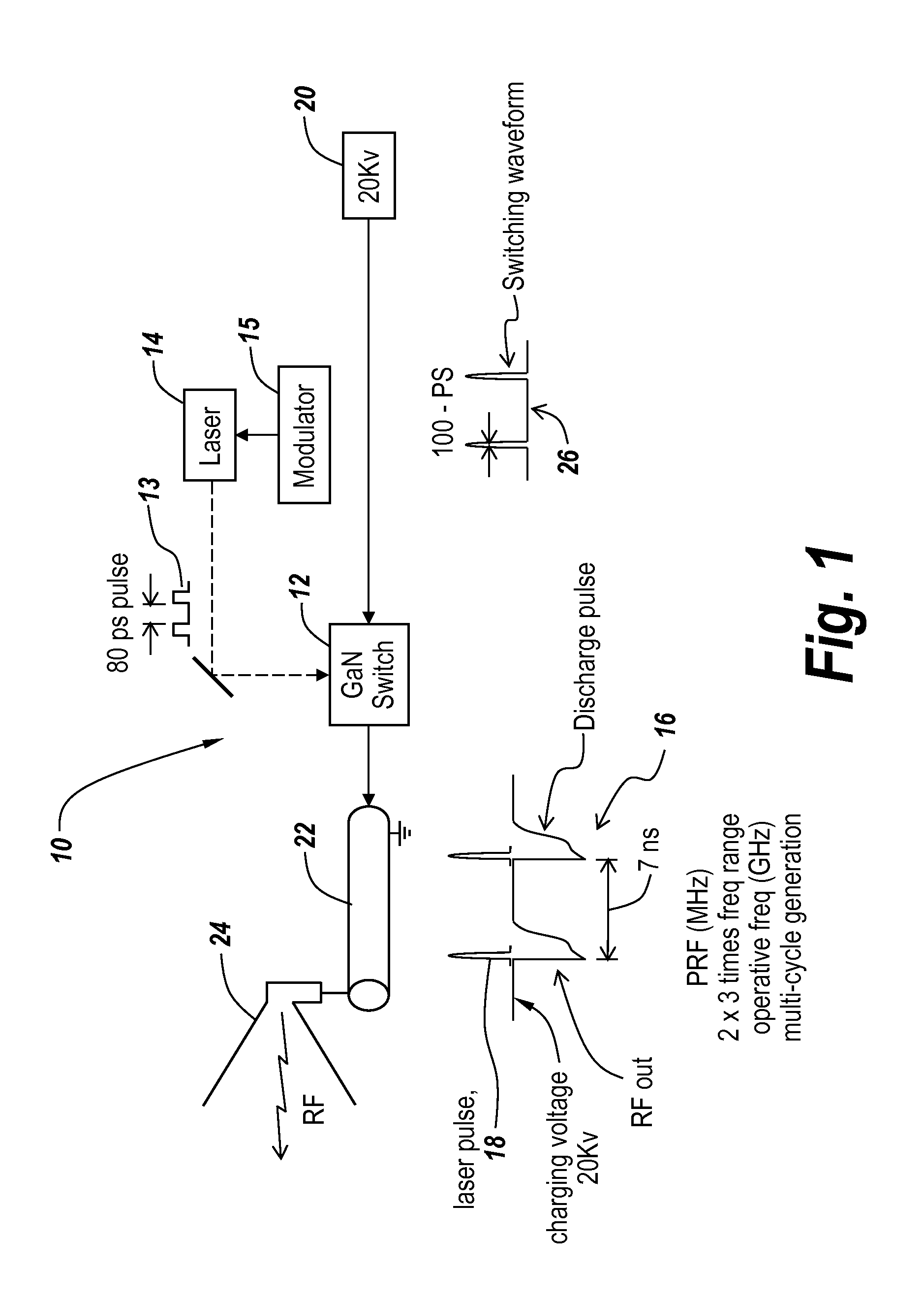
The present patent provides a system and method for generating high-power RF waves using a photoconductive switch. The system includes a laser to activate the switch, a pulse forming network to discharge the transmission line, and a high-voltage source. The method involves charging the transmission line and then discharging it to ground using the photoconductive switch. The technical effects include a highly flexible and fast response time for the photoconductive switch, which makes it possible to generate high-power RF waves with a high precision.

Problems solved by technology

Electronic warfare involves a generation of high-power RF pulses which are incident on target radars / receivers so as to either result in jamming or to in fact cause massive malfunctions of the receiving apparatus.
The problem with such silicon technology is primarily the long carrier lifetime which limits the repetition rate and thus the frequency of the RF output as well as the ability to specifically tailor the outgoing RF waveform.
Moreover, silicon technology has a limited voltage holding capability that limits output power and also offers only a limited tuning capability.
Thus, photoconductive switch-based RF waveform generators based on silicon are limited to frequencies in the kilohertz pulse repetition rate range and are further restricted by the limits on the high-voltage supply.
Additionally, the silicon-based photoconductive switch RF generators are not capable of putting enough energy on a target unit, either because the RF output pulses are not powerful enough or because these systems cannot rapidly fire RF pulses on target.
With silicon technology the building up of pulses to be fired in rapid succession on a target is simply not possible.
For instance, it is not possible, utilizing silicon switches, to generate multiple high-power pulses in a single, rapid burst.
Further, due to the fact that only a single output pulse can be generated with silicon switching systems every 10 to 100 μs, there is no possibility to provide additional laser shots within this 10 to 100 μs silicon switch recovery time., i.e. prior to the completion of the initial transmission line discharge phase.

Method used


Image

  • Generation of Flexible High Power Pulsed Waveforms
  • Generation of Flexible High Power Pulsed Waveforms
  • Generation of Flexible High Power Pulsed Waveforms

Examples


Embodiment Construction

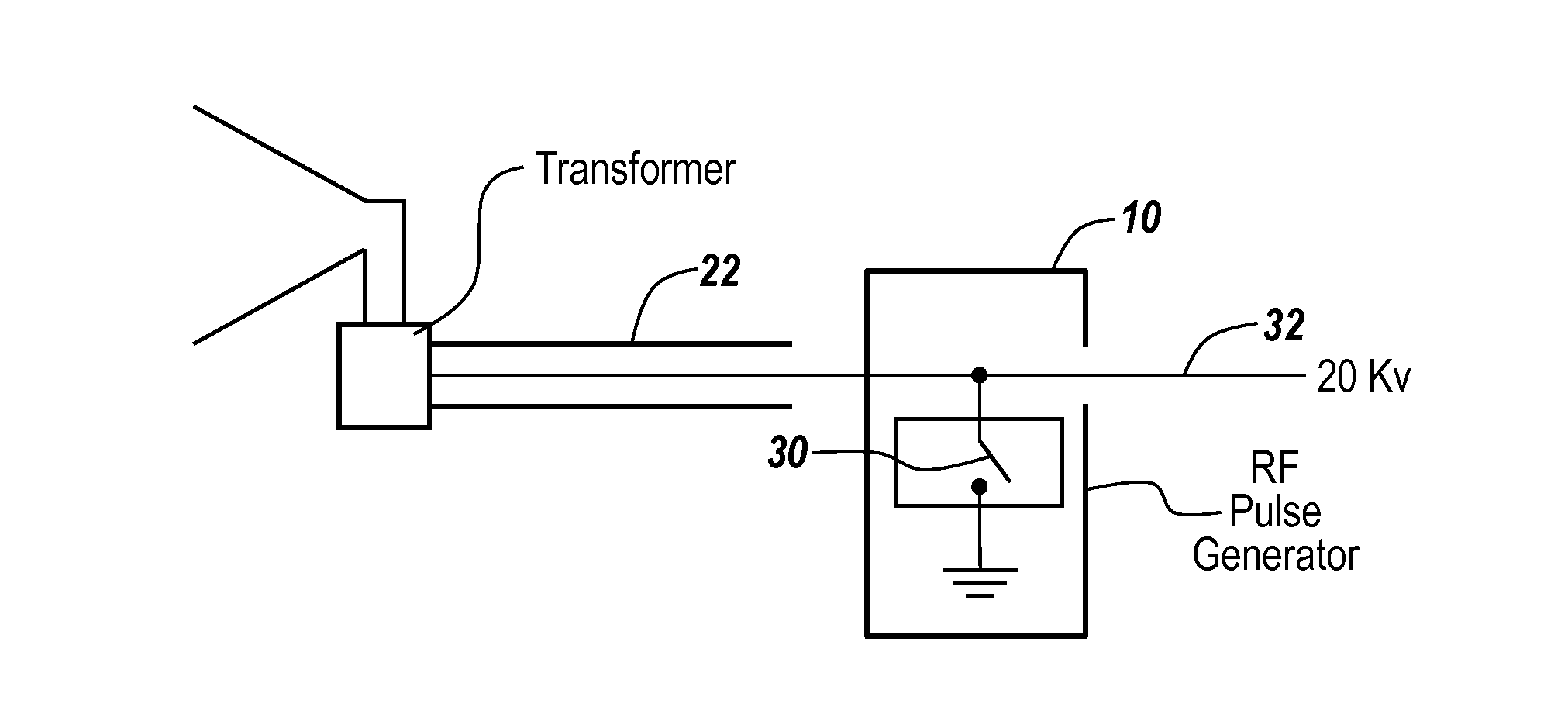
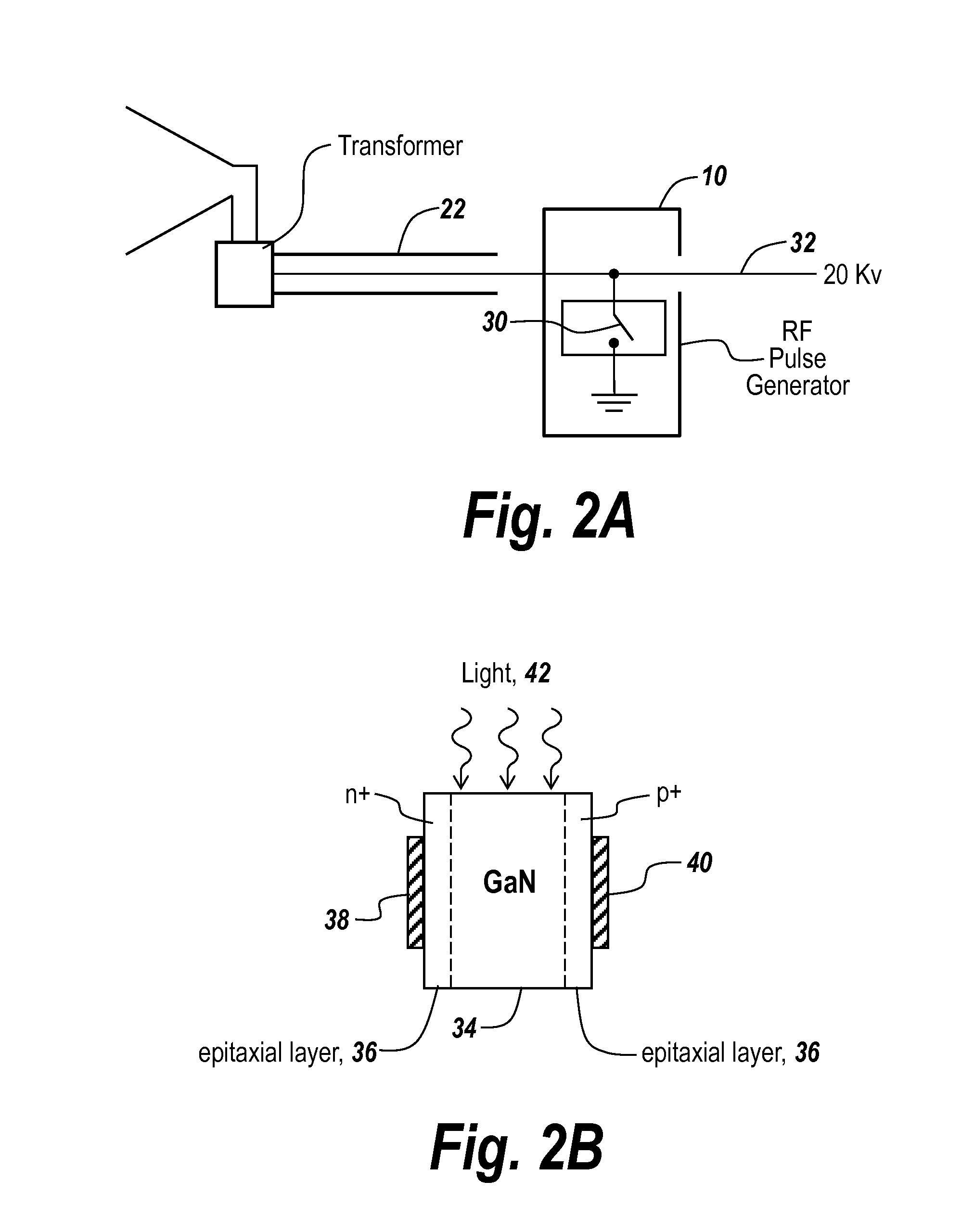
[0027]In order to provide a waveform flexible photoconductive switch-based RF generator, the photoconductive switch is a sub nanosecond response time switch based on gallium nitride technology which has as its primary characteristic short carrier lifetimes, as well as substantially increased voltage holding. This in turn results in the ability to tune the RF waveform over relatively wide frequency range. Moreover, the moderate on—resistance characteristic of the gallium nitride is overcome by the 20 kV capability of the switch. Because of the physics within the gallium nitride crystal, one can rapidly switch 100,000 times faster than a silicon switch so that one can manage to change the frequency that comes out without having to change the transformer utilized between the pulse generator and an associated antenna.

[0028]Because of the ability to rapidly cycle the gallium nitride switch, it is possible for a charged transmission line to be multiply discharged prior to the time that al...


PUM


Abstract

A method for generating high power pulsed RF waveforms comprises the steps of charging a transmission line in a pulse forming network with a high-voltage and discharging the voltage on the transmission line to ground utilizing a gallium nitride photoconductive switch.

Description

FIELD OF DISCLOSURE[0001]This invention relates to the generation of flexible, high power pulsed waveforms, and more particularly to the utilization of a gallium nitride photoconductive switch to achieve this flexibility.BACKGROUND OF THE DISCLOSURE[0002]Electronic warfare involves a generation of high-power RF pulses which are incident on target radars / receivers so as to either result in jamming or to in fact cause massive malfunctions of the receiving apparatus. It has been the goal of those involved in electronic warfare to be able to put a considerable amount of energy on a target and to tailor the energy both in frequency and in pulse repetition rate to match that of the target's vulnerabilities. Target radars are now considerably more sophisticated and operate on the basis of coded signatures so as to be able to defeat jamming systems by being able to filter out indiscriminate jamming that doesn't take into account the sophistication of the target radar. Also, in communication...

Claims


Application Information

Patent Timeline
IPC IPC(8): H01L31/0304H01L31/09H03K17/78
CPCH01L31/03044H01L31/09H03K17/78H01L31/08Y02E10/544
Inventor KOZYREV, ALEXANDERMCGEEHAN, JOHNMOREL, YANNICK
Owner BAE SYST INFORMATION & ELECTRONICS SYST INTERGRATION INC
Learn More