Plasma processing apparatus and plasma processing method

a plasma processing and plasma technology, applied in electrical apparatus, semiconductor/solid-state device testing/measurement, electric discharge tubes, etc., can solve the problems of generating voltage breakdown of electrostatic chucking film, risk of reducing electrostatic chucking force, etc., and achieve high-quality effects

Active Publication Date: 2016-07-14
HITACHI HIGH-TECH CORP
View PDF2 Cites 80 Cited by
  • Summary
  • Abstract
  • Description
  • Claims
  • Application Information

AI Technical Summary

Benefits of technology

[0023]Among the inventions disclosed in the application, the advantageous effects obtained by the representatives will be briefly explained as below.
[0024]It is possible to perform the plasma processing with high quality.BRIEF DESCRIPTIONS OF THE DRAWINGS
[0025]FIG. 1 is an explanatory diagram illustrating an example of a configuration of a main section in a plasma processing apparatus using a bipolar type electrode according to an embodiment;
[0026]FIG. 2 is a timing chart illustrating an example of a signal of each unit of the plasma processing apparatus in which temperature control of a semiconductor wafer is difficult at the time of only using a monitor value of a radio-frequency voltage, which is a bias voltage of a high power side, to be applied to an ESC electrode examined by the present inventors;
[0027]FIG. 3 is a timing chart illustrating an example of a signal of each unit of the plasma processing apparatus in which an electrostatic chucking film is dielectrically broken down at the time of only using the monitor value of the radio-frequency voltage, which is the bias voltage of the high power side, to be applied to the ESC electrode examined by the present inventors;
[0028]FIG. 4 is a timing chart illustrating an example of a signal timing of each unit in the plasma processing apparatus of FIG. 1;

Problems solved by technology

As a result, there is a risk of decrease in electrostatic chucking force and generation of voltage breakdown of an electrostatic chucking film.

Method used


Image

  • Plasma processing apparatus and plasma processing method
  • Plasma processing apparatus and plasma processing method
  • Plasma processing apparatus and plasma processing method

Examples


example 1

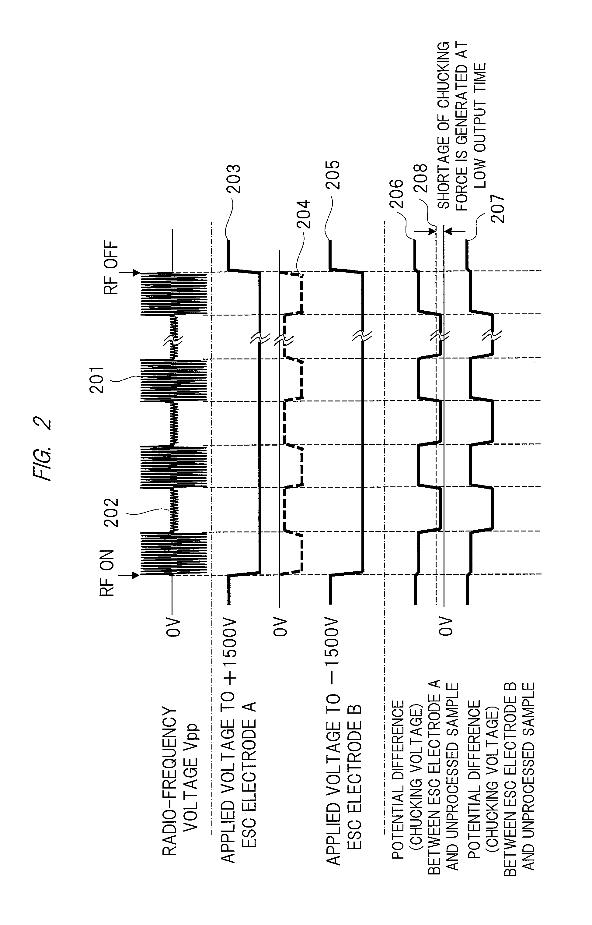
[0099]For example, it is considered a case in which Vpp_H=4000 V and Vpp_L=0 V are monitored with respect to the recipe set values of VESC=3000 V, R1=0.45 and D=80% while using the ESC electrode having the threshold value Vd=3000 V.

[0100]A voltage of the ESC at the high voltage time is that a voltage of ECS(+) is 60 V from Equation 7, a voltage of ESC(−) is −2940 V from Equation 8, and a voltage at the high voltage time of the TM bias is −1800 V from Equation 3 of the CW time. Further, a voltage between the ESC electrode at the high voltage time and the unprocessed sample is |1860 / 1140 V|, and a voltage between the ESC electrode at the low voltage time and the unprocessed sample is |60 / 2940 V| from Equations 9 and 10, so that the voltage goes below the threshold value Vd, and thus, does not cause an error to restrict the use, that is, a withstand voltage failure of the electrostatic chucking film.

[0101]When Vpp=5000 V, however, a voltage between the ESC electrode at the high voltage...

example 2

[0105]In addition, although the example regarding the bipolar type electrode has been illustrated in the above-described mode of Example 1, the application to the unipolar type electrode is also possible. FIG. 6 is an explanatory diagram illustrating another example of the configuration of the main section in the plasma processing apparatus of FIG. 1.

[0106]In FIG. 6, an unprocessed sample installation unit 600 includes a base material section 601, an electrostatic chucking film 602, and an ESC electrode 603. The electrostatic chucking film 602 is placed on an upper part of the base material section 601 to which radio-frequency power is applied.

[0107]The electrostatic chucking film 602 is formed using ceramic, for example. In addition, the ESC electrode 603 is embedded in the electrostatic chucking film 602. A low pass filter 606 is connected to the ESC electrode 603, and an ESC power supply 605 is connected to the low pass filter 606.

[0108]The ESC power supply 605 serving as the DC ...


PUM

PropertyMeasurementUnit
radio-frequency voltagesaaaaaaaaaa
frequencyaaaaaaaaaa
TM frequencyaaaaaaaaaa

Abstract

To control temperature of a sample in plasma processing with high accuracy while securing an electrostatic chucking force without breakdown of an electrostatic chucking film.When radio-frequency power is time modulated, a high-voltage side Vpp detector detects a first voltage value which is a peak-to-peak voltage value of a radio-frequency voltage applied to a sample stage in a first period of the time modulation having a first amplitude. A low-voltage side Vpp detector detects a second voltage value which is a peak-to-peak voltage value of a radio-frequency voltage applied to the sample stage in a second period having a second amplitude smaller than the first amplitude. Then, an ESC power supply control unit controls output voltages from ESC power supplies based on the first voltage value, the second voltage value and a duty ratio of the time modulation.

Description

CROSS-REFERENCE TO RELATED APPLICATION[0001]The present application claims priority from Japanese Patent Application No. 2015-002723 filed on Jan. 9, 2015 and No. 2015-200701 filed on Oct. 9, 2015, the contents of which are hereby incorporated by reference into this application.TECHNICAL FIELD OF THE INVENTION[0002]The present invention relates to a plasma processing apparatus and a plasma processing method, and particularly to a technique which is effective for control of damage on an electrode of a plasma processing apparatus caused by increase of plasma potential.BACKGROUND OF THE INVENTION[0003]A structure in which a semiconductor wafer is electrostatically chucked, and helium gas is caused to flow between the semiconductor wafer and en electrode has been widely used as a technique for accurately securing temperature of the semiconductor wafer in a plasma processing apparatus such as a plasma etching apparatus.[0004]Two systems of unipolar (monopole) and bipolar (dipole) systems...

Claims


Application Information

Patent Timeline
Patent Type & Authority Applications(United States)
IPC IPC(8): H01J37/32H01L21/683H01L21/66H01L21/67
CPCH01J37/32935H01J37/32082H01J37/32715H01J37/32706H01J2237/336H01L21/6833H01L21/67253H01L22/20H01J2237/334H01L21/67069H01L21/67248H01L21/6831
Inventor ARASE, TAKAOMORI, MASAHITOYOKOGAWA, KENETSUTAKEGAWA, YUUSUKEICHINO, TAKAMASA
Owner HITACHI HIGH-TECH CORP
Why Eureka
Try Eureka