Method of plasma-enhanced atomic layer etching
a technology of atomic layer and etching, which is applied in the direction of basic electric elements, electrical equipment, electric discharge tubes, etc., can solve the problems of low etching rate, poor controllability of etching direction, and need to improve, so as to increase the efficiency of purging
- Summary
- Abstract
- Description
- Claims
- Application Information
AI Technical Summary
Benefits of technology
Problems solved by technology
Method used
Image
Examples
example 13
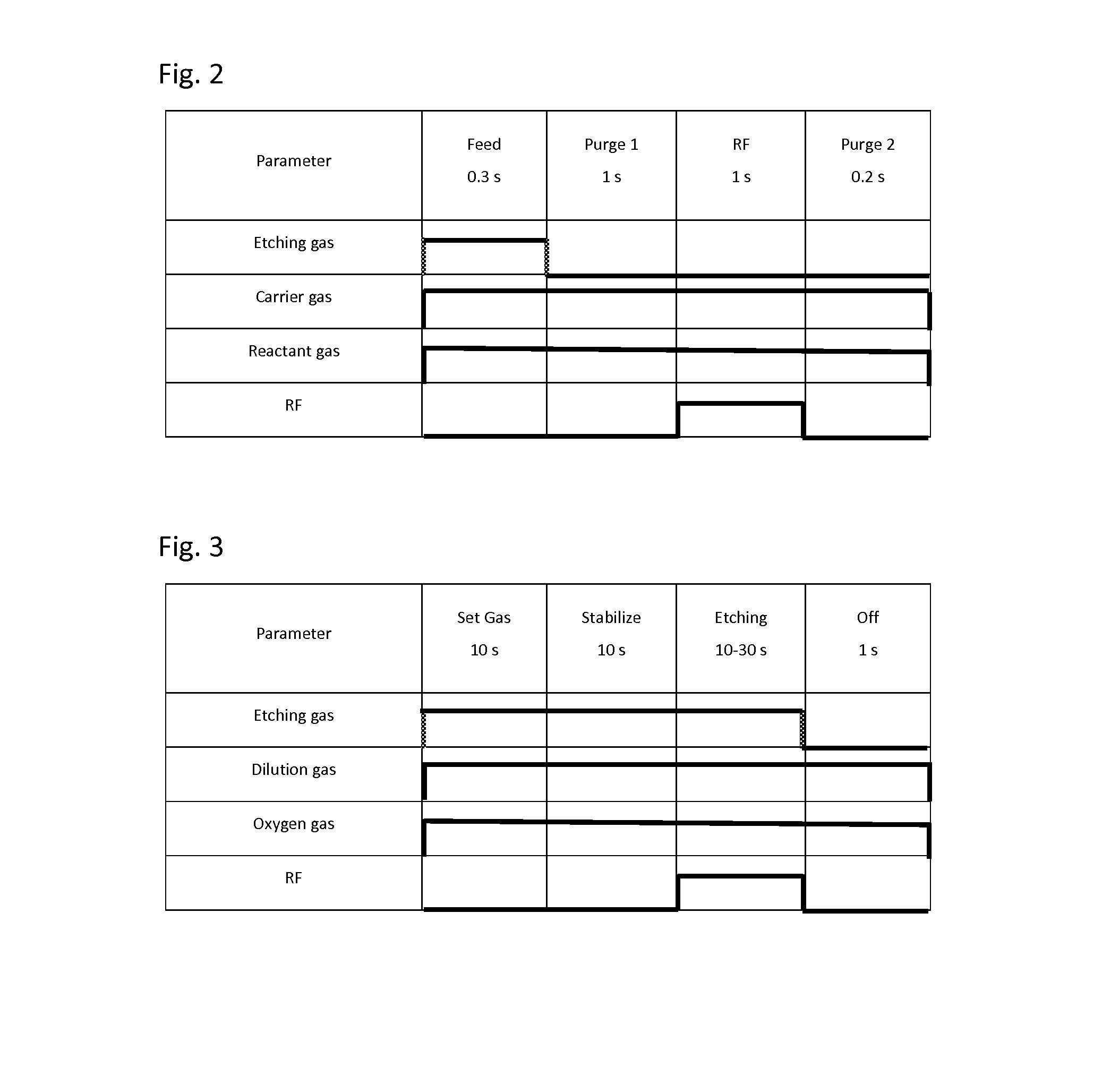
[0050]The ALE process was performed according to Example 5 above, except that the feed time of etching gas was changed. FIG. 4 is a graph showing the relationship between etching rate per cycle (EPC) (nm / cycle) and etching gas feed time per cycle (seconds). As shown in FIG. 4, after the feed time reached 0.2 seconds, EPC was unchanged, indicating that self-limiting adsorption reaction process was conducted.
example 14
[0051]The ALE process was performed according to Example 5 above, except that the purge time upon feeding of the etching gas was changed. FIG. 5 is a graph showing the relationship between etching rate per cycle (EPC) (nm / cycle) and purge time per cycle (seconds). As shown in FIG. 5, after the purge time reached 0.5 seconds, EPC was unchanged, indicating chemisorption of the etching gas was conducted.
PUM
 Abstract
Description
Claims
Application Information


