
Epitaxial Hexagonal Materials on IBAD-Textured Substrates

a hexagonal material and substrate technology, applied in semiconductor/solid-state device manufacturing, semiconductor devices, electrical equipment, etc., can solve the problems of cost of led luminaire systems, unable to completely replace incandescent and fluorescent lighting, and far from a mainstream application in commercial lighting

Active Publication Date: 2016-08-11
IBEAM MATERIALS INC
View PDF3 Cites 5 Cited by
  • Summary
  • Abstract
  • Description
  • Claims
  • Application Information

AI Technical Summary

Benefits of technology

The present invention relates to a method for growing epitaxial materials on a substrate using an ion-beam assisted deposition (IBAD) texturing process. This method allows for the use of flexible metal foil substrates, which can be easily obtained and used for electronic device fabrication. The invention also includes a method for reducing the cost of LED lighting systems by eliminating the need for surface mounted devices (SMDs) and pick-and-place technology. The text also discusses the issue of scale in manufacturing LED chips and packages, and proposes a solution to reduce costs by increasing the substrate size incrementally from 2-inch to 6-inch single-crystal wafers.

Problems solved by technology

However, the greatest barrier still holding back LEDs from completely replacing incandescent and fluorescent lighting is cost of the LED luminaire systems.
Although LED lighting has made great strides in penetrating the lighting market, it is currently mostly focused in the niche high-end lighting space and still far from a mainstream application in commercial lighting where it is hard to compete in cost with simple fluorescent tubes.
For LEDs to dominate the whole lighting market the cost of LED lighting will still have to come down by several orders of magnitude.
This is in spite of the fact that the LED chip and package costs have already come down incredibly by several orders of magnitude in the past decade.
However, single-crystal substrates are typically rigid, expensive, and readily available in diameters of only less than 100 mm, except for silicon wafers.
Limiting the growth of GaN to lattice-matched single-crystal substrates reduces the number of practical substrates to sapphire (Al2O3), SiC, and bulk-GaN, which can be expensive and unavailable in large sizes.
Thus far it has not been possible to grow single-crystal GaN directly on metal or other non-oriented substrates due to the lack of epitaxial registry.
Previous IBAD texturing in fluorites was not developed, not easy to work with, and the IBAD texture widths were more than 15° in-plane FWHM.
Thus IBAD (111) was not thought to be of sufficient quality to produce high-quality semiconductor materials with in-plane alignment of <1°.
Thus typical semiconductor materials on IBAD are of inferior quality for devices and cannot compete with semiconductors on single crystal substrates.
Good quality LED and other devices have not been produced.
Several previous attempts to make GaN devices have been unsuccessful, since the materials have not been of high enough quality in terms of crystalline perfection and carrier mobility.

Method used


Image

  • Epitaxial Hexagonal Materials on IBAD-Textured Substrates
  • Epitaxial Hexagonal Materials on IBAD-Textured Substrates
  • Epitaxial Hexagonal Materials on IBAD-Textured Substrates

Examples


example 1

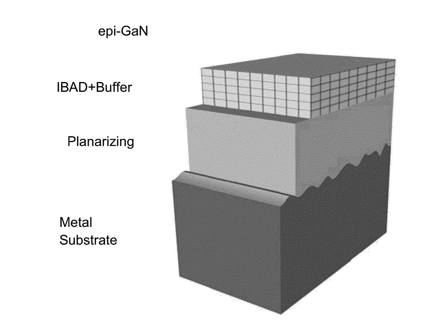
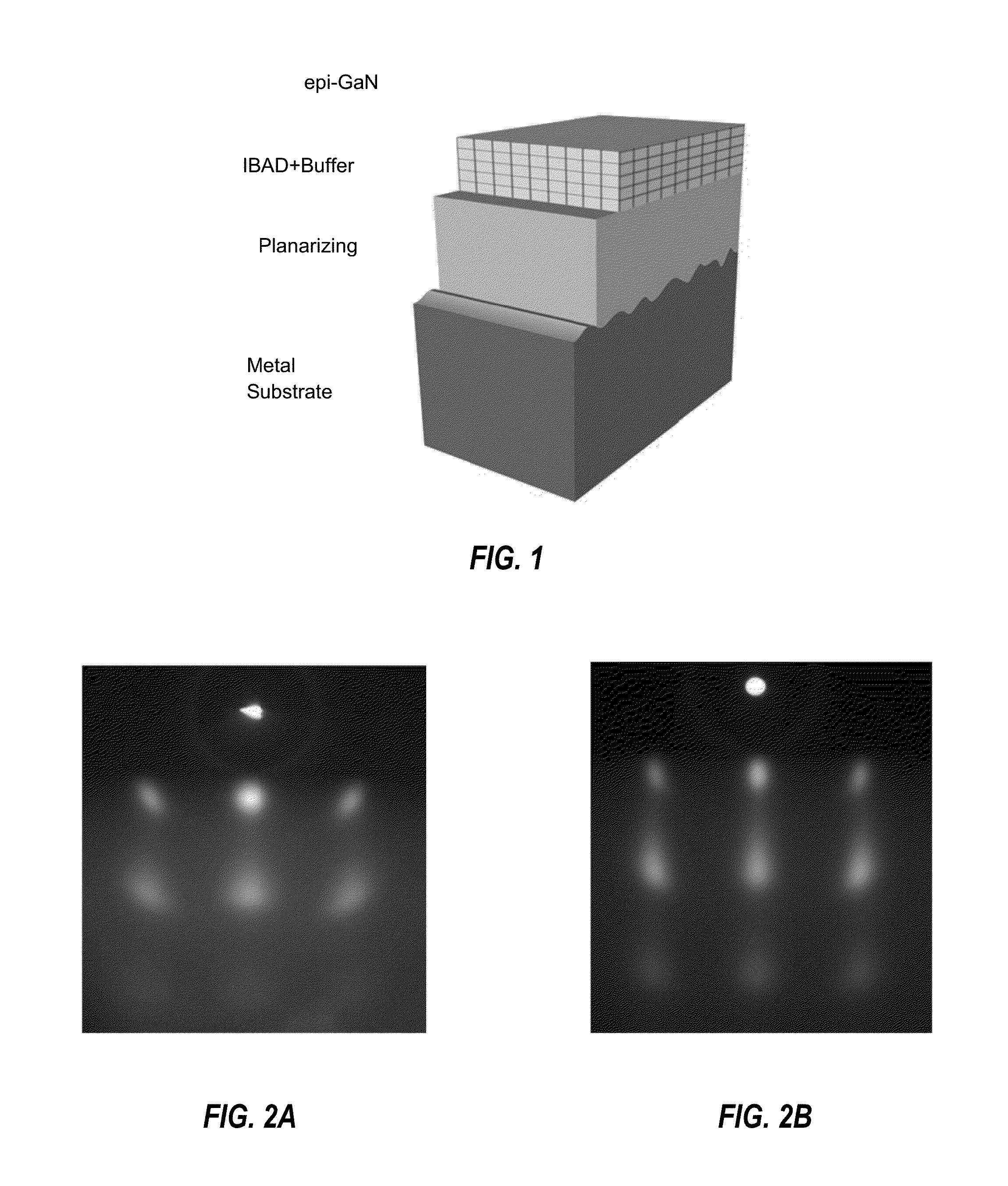
[0061]To demonstrate the applicability of IBAD templates for epitaxial growth of GaN and related group III nitride materials, MOCVD growth of GaN, also known as MOVPE (metal-organic vapor phase epitaxy), was performed. Samples were briefly heated to 800-1000° C. in flowing H2 prior to growth. The GaN nucleation layer was grown using trimethylgallium (TMGa) and ammonia (NH3) using H2 and N2 push flows at a substrate temperature of 530° C. After the growth of the GaN NL, the TMGa was turned off and the wafers were ramped in temperature to 1050° C. over 8 minutes. At 1050° C. the TMGa was turned on for 1 hour resulting in ≦2 μm of GaN film. After growth the wafers were cooled in the NH3, H2, and N2 flows and removed from the growth reactor.

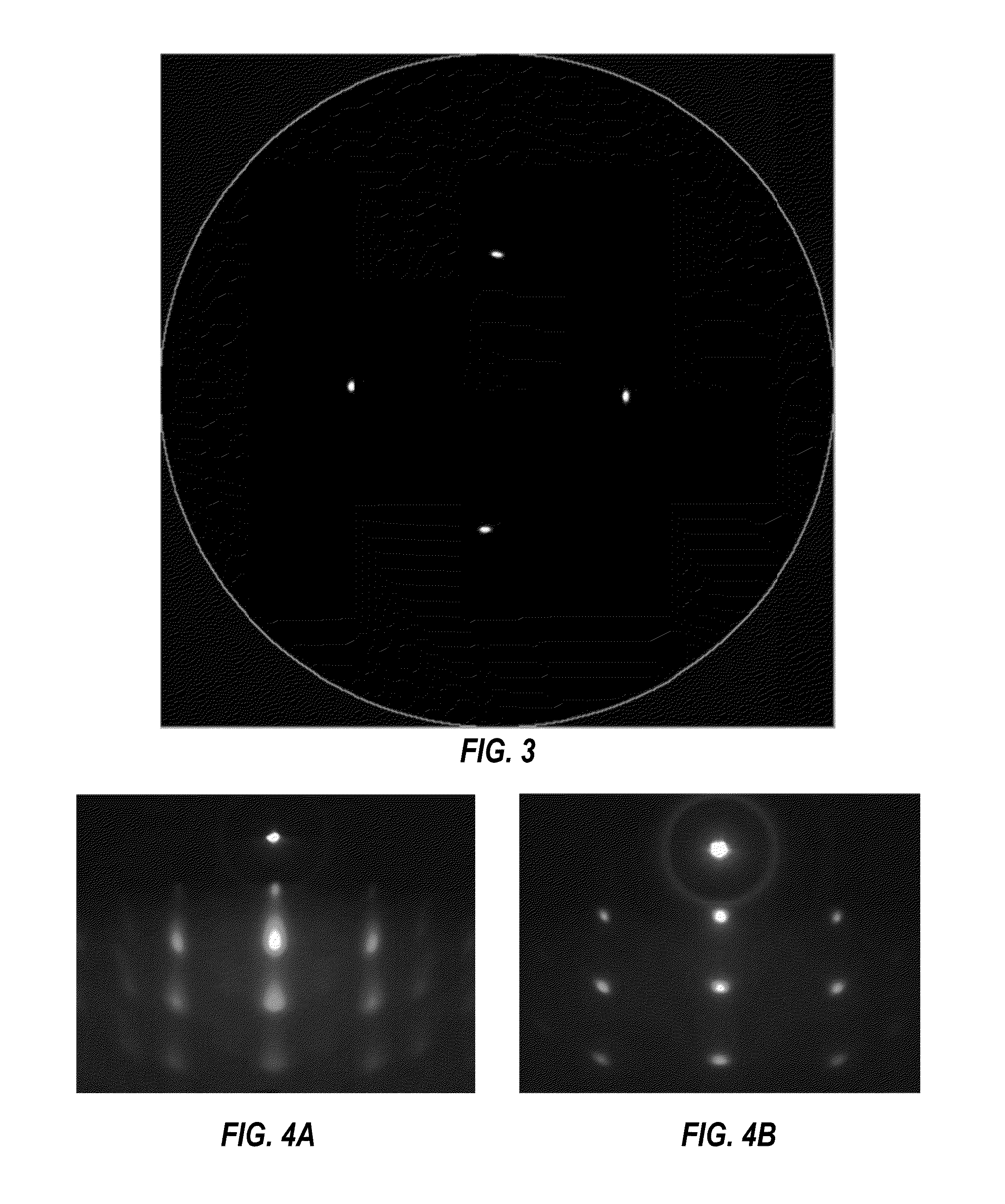
[0062]For the templates for GaN growth, substrates were prepared separately prior to GaN growth. In one embodiment we utilized IBAD-textured MgO films. These films are oriented with the (100) axis out of the plane and form a square, 4-fold symmetric ...

example 2

[0073]A thick layer of GaN was deposited on an IBAD template. Typically GaN is 4 to 6 micrometers in thickness, the top part of which is n-doped with Si, as can be seen in FIG. 25. As shown in FIG. 26, on top of the GaN layer an LED structure pn junction is grown, together with a multi-quantum well (MQW) structure, which is a multilayer of 5 alternating InGaN and GaN layers. On top of the MQW is p-doped electron blocking layer followed by the p-GaN doped with Mg. Such a heterostructure is standard for making LEDs in industry.

[0074]Performance of such an LED device was measured as compared to LEDs prepared on single-crystal sapphire, which is a standard substrate in industry. Results are shown in FIGS. 27-29. Comparisons were done with photoluminescence (PL) (shining a light on the device), and electroluminescence (EL) (passing a current through the device), light measurements. For the first devices fabricated PL shows between 10 and 40% of light in IBAD LEDs compared to standard sap...


PUM

PropertyMeasurementUnit
temperatureaaaaaaaaaa
deposition timeaaaaaaaaaa
roughnessaaaaaaaaaa

Abstract

A multilayer structure including a hexagonal epitaxial layer, such as GaN or other group III-nitride (III-N) semiconductors, a <111> oriented textured layer, and a non-single crystal substrate, and methods for making the same. The textured layer has a crystalline alignment preferably formed by the ion-beam assisted deposition (IBAD) texturing process and can be biaxially aligned. The in-plane crystalline texture of the textured layer is sufficiently low to allow growth of high quality hexagonal material, but can still be significantly greater than the required in-plane crystalline texture of the hexagonal material. The IBAD process enables low-cost, large-area, flexible metal foil substrates to be used as potential alternatives to single-crystal sapphire and silicon for manufacture of electronic devices, enabling scaled-up roll-to-roll, sheet-to-sheet, or similar fabrication processes to be used. The user is able to choose a substrate for its mechanical and thermal properties, such as how well its coefficient of thermal expansion matches that of the hexagonal epitaxial layer, while choosing a textured layer that more closely lattice matches that layer.

Description

CROSS-REFERENCE TO RELATED APPLICATIONS[0001]This application claims priority to and the benefit of the filing of U.S. Provisional Patent Application Ser. No. 62 / 114,504, entitled “IBAD-Textured Substrates for Growth of Epitaxial Group-III Nitride Materials and Method of Making the Same”, filed on Feb. 10, 2015, and U.S. Provisional Patent Application Ser. No. 62 / 262,815, entitled “IBAD-Textured Substrates for Growth of Epitaxial Group-III Nitride Materials and Method of Making the Same”, filed on Dec. 3, 2015, and the specification and claims thereof are incorporated herein by reference.FEDERALLY SPONSORED RESEARCH OR DEVELOPMENT[0002]The U.S. Government has a paid-up license in this invention and the right in limited circumstances to require the patent owner to license others on reasonable terms as provided for by the terms of Assistance Agreement No. AR0000447 awarded by the U.S. Department of Energy's Advanced Research Projects Agency-Energy.BACKGROUND OF THE INVENTION[0003]1. F...

Claims


Application Information

Patent Timeline
Patent Type & Authority Applications(United States)
IPC IPC(8): H01L33/32H01L33/18
CPCH01L33/18H01L33/32H01L33/02H01L33/16H01L21/02458H01L21/02483H01L21/02488H01L21/02502H01L21/02516H01L21/0254H01L27/15H10K59/00
Inventor MATIAS, VLADIMIRYUNG, CHRISTOPHER
Owner IBEAM MATERIALS INC
Learn More