Large power circuit and manufacturing method thereof

a technology of power circuit and manufacturing method, applied in non-linear optics, instruments, optics, etc., can solve the problems of negative liquid crystal molecules, no tolerance for rub process, related issues, etc., and achieve the effect of improving the utilization ratio of glass substrate, reducing the requirements of cvd apparatus, and improving the effect of benefits

Inactive Publication Date: 2016-08-18
TCL CHINA STAR OPTOELECTRONICS TECH CO LTD
View PDF2 Cites 3 Cited by
  • Summary
  • Abstract
  • Description
  • Claims
  • Application Information

AI Technical Summary

Benefits of technology

[0038]The benefits of the present invention are: distances between the power circuit (metal pattern) and edges of the lower substrate become larger, and the requirements for CVD apparatus can be reduced; the occupied area of the power circuit on the lower substrate is reduced, and it is beneficial to achieve a better usage ratio of a glass substrate to obtain better benefits; an overlapping area of wirings of the lower substrate is reduced to eliminate the occurrence possibility of electrostatic damage.

Problems solved by technology

Significantly, almost no tolerance can exist for the rub process.
From time to time, related issues happen during a massive manufacture production.
However, related issues remain: the negative liquid crystal molecules 114 in certain area around the ribs 115 cannot be aligned vertically so well.
Even right in front of the panel, larger light leak may occur to affect the promotion of the contrast ratio property of the Multi-domain Vertical Alignment.
Nevertheless, the foregoing two technologies still possess another problem.
The power circuit and particular the power alignment circuit of the common PSVA is located at the edge of the large substrate and leads to the problems below:
The longer the power circuit is, the more chance that the electrostatic damage happens; the conditions of wiring crossing cannot be avoided under circumstance of long wirings.
At the cross sections of the wirings, the electrostatic breakdown can easily happen.
Consequently, the right voltage cannot be applied to the liquid crystal cell for the liquid crystal cell.
Such wasted products may exist and affect the yield of the products;
It goes against improvement of the glass substrate usage ratio and reduction of the manufacture cost.
In a manufacture competition, it is put at a disadvantage;
3. The power terminals of the power circuit are generally located at the edge of the large lower substrate, which is close to the edge of film formation area of CVD. In the manufacture processes, these metal terminals are demanded to be packaged except in the desired opens for guaranteeing no damage to the terminals in the entire manufacture process. For preventing the acid alkali corrosions to the metal terminals and the electrochemical corrosion in the long-term placement. The CVD equipment is requested to provide the film formation area closer to the edges. However, the formation of the dielectric film depends on the film formation ability of the CVD equipment. An over requirement can cause the increase of the equipment cost.

Method used


Image

  • Large power circuit and manufacturing method thereof
  • Large power circuit and manufacturing method thereof
  • Large power circuit and manufacturing method thereof

Examples


first embodiment

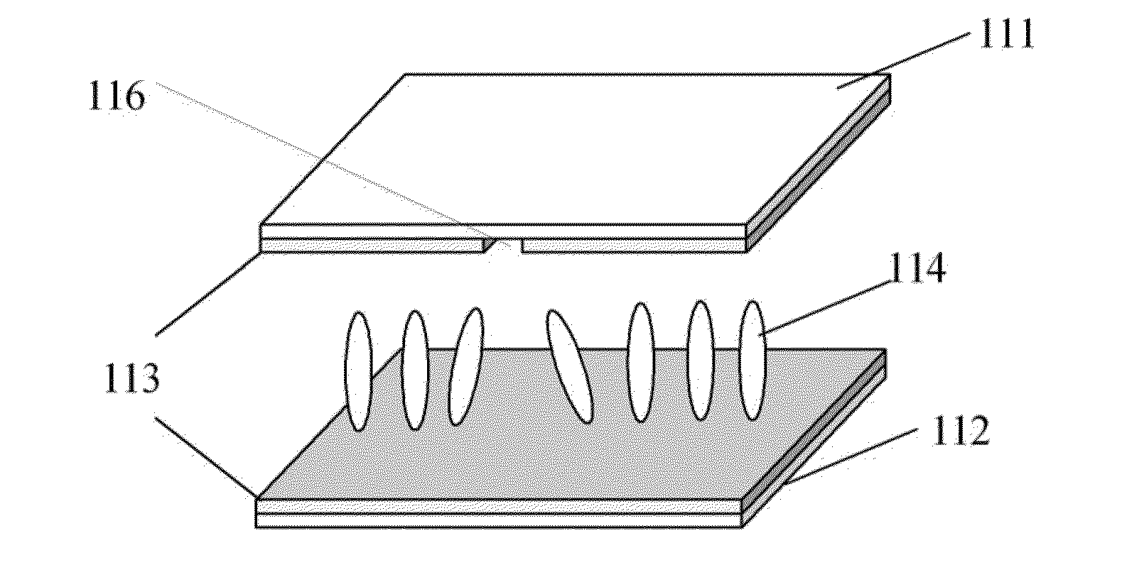
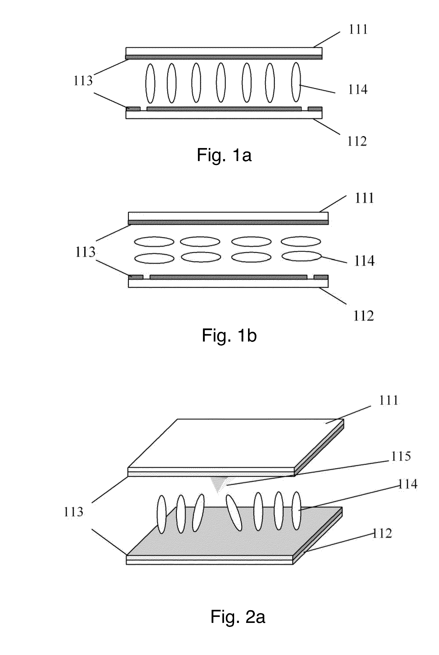
[0081]As shown in FIG. 6, which is a sectional diagram of an array substrate according to the present invention, the manufacture process of the lower substrate (array substrate) is described below:

[0082]manufacturing a gate metal layer on the glass substrate 60 with a sputter apparatus;

[0083]obtaining a gate pattern 61 with exposure, development and etching;

[0084]manufacturing a dielectric film 62 and an amorphous silicon 63 with a CVD apparatus;

[0085]obtaining a silicon island 64 with exposure, development and etching;

[0086]manufacturing a source / a drain metal layer with a sputter apparatus;

[0087]obtaining a source / a drain pattern 65 with exposure, development and etching;

[0088]manufacturing a dielectric film 66 with a CVD apparatus;

[0089]removing dielectric film at the thin film transistor and other necessary locations with exposure, development and etching to reveal the metal below to manufacture contact holes;

[0090]manufacturing a pixel electrode / a common electrode 67.

[0091]The ...

second embodiment

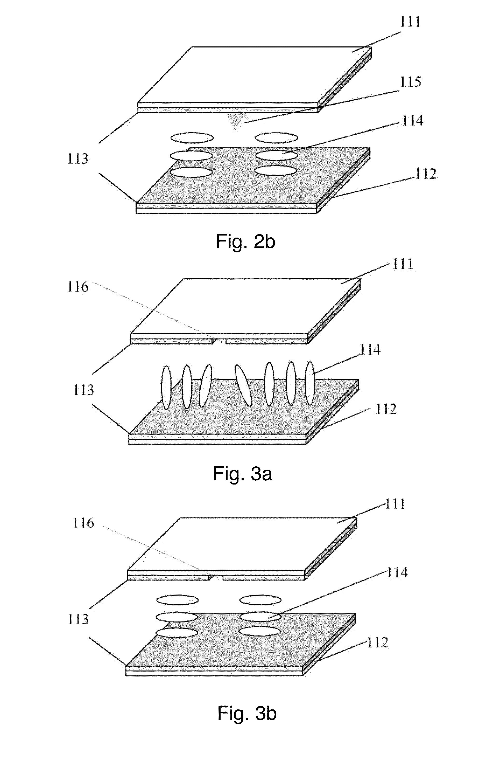
[0101]As shown in FIG. 10, which is a sectional diagram of an array substrate according to the present invention, the manufacture process of the lower substrate (array substrate) is described below:

[0102]manufacturing a gate metal layer with a sputter apparatus;

[0103]obtaining a gate pattern 101 with exposure, development and etching;

[0104]manufacturing a dielectric film 102 and an amorphous silicon 103 with a CVD apparatus;

[0105]obtaining a silicon island 104 with exposure, development and etching;

[0106]manufacturing a source / a drain metal layer with a sputter apparatus;

[0107]obtaining a source / a drain pattern 105 with exposure, development and etching;

[0108]manufacturing a dielectric film 106 with a CVD apparatus;

[0109]sequentially manufacturing a red blocking pattern, a green blocking pattern and a blue blocking pattern to form the color filter 107;

[0110]manufacturing a dielectric film 108 with a CVD apparatus;

[0111]removing dielectric film at the thin film transistor and other n...


PUM

PropertyMeasurementUnit
widthsaaaaaaaaaa
poweraaaaaaaaaa
transparentaaaaaaaaaa

Abstract

The present invention provides a large power circuit and a manufacture method thereof. The large power circuit comprises a color filter substrate and an array substrate which are opposed, and a floating ITO pattern is positioned in an outer region of the color filter substrate, and contact holes are positioned in an outer region of the array substrate where is close to an inner region of the array substrate, and the contact holes are electrically connected to wirings in the inner region of the array substrate, and positions of the contact holes match with the floating ITO pattern, and conductors are located between the contact holes and the floating ITO pattern for conducting electric currents. The present invention also provides a corresponding manufacture method of the large power circuit. The requirements for CVD apparatus can be reduced according to the large power circuit and the manufacture method thereof of the present invention. It is beneficial to achieve a better usage ratio of a glass substrate to obtain better benefits and eliminate the occurrence possibility of electrostatic damage.

Description

FIELD OF THE INVENTION[0001]The present invention relates to a display skill field, and more particularly to a large power circuit design and a manufacture method thereof.BACKGROUND OF THE INVENTION[0002]With the development of the world constructed by information, the requirements of display device have been growing. For satisfying such requirements, the recent panel display devices, such as a liquid crystal display (LCD), a plasma display panel (PDP) and an Organic Light-Emitting Diode (OLED) display have been developing so rapidly. In these panel display devices, the LCD has gradually replaced the cathode ray tube (CRT) display device with its advantages, light weight, small volume and low power consumption.[0003]In the early stage, Twisted Nematic (TN) or Super Twisted Nematic (STN) LCD displays which have developed first possess issues of low contrast ratio and narrow view angle. With the advance in living standard, more and higher demands appear to the display devices. Consequ...

Claims


Application Information

Patent Timeline
Patent Type & Authority Applications(United States)
IPC IPC(8): G02F1/1335G02F1/1339G02F1/1343
CPCG02F1/1333G02F1/1343G02F1/133512G02F2001/133302G02F1/13394G02F1/13439G02F1/133514G02F1/13452G02F1/13454G02F1/133302
Inventor LIAO, BINGJEIXU, LIANGMA, JIAXINGCHEN, CHAOMU
Owner TCL CHINA STAR OPTOELECTRONICS TECH CO LTD
Why Eureka
Try Eureka