Touch substrate and touch screen

a substrate and touch technology, applied in the field of touch technology, can solve the problems of low signal-noise ratio, high resistance of ito, affecting the touch effect, etc., and achieve the effects of reducing the distance between adjacent metal meshes, increasing the capacitance between electrodes, and increasing the signal-noise ratio

Active Publication Date: 2016-08-25
BOE TECH GRP CO LTD +1
View PDF15 Cites 16 Cited by
  • Summary
  • Abstract
  • Description
  • Claims
  • Application Information

AI Technical Summary

Benefits of technology

[0013]In the touch substrate of the present invention, at least one edge of each of the metal meshes is provided with the side strip, so that opposite areas between adjacent metal meshes are increased (or the distance between the adjacent metal meshes is reduced), thus the capacitance between the electrodes is increased, then the signal-noise ratio may be increased, the touch effect may be improved and the existing touch chip may be applied.

Problems solved by technology

However, the resistance of ITO is high, which may affect the touch effect.
However, the solution in which the driving metal meshes 11 and the sensing metal meshes 21 are provided in the same layer may bring about some problems, as shown in FIG. 1, a capacitance is mainly formed between the driving electrode 1 and the sensing electrode 2 by adjacent side surfaces of the driving electrode 1 and the sensing electrode 2 (in other words, edges of the metal meshes).
However, the areas of the side surfaces of the metal meshes are very small, and when a driving electrode 1 and a sensing electrode 2 are adjacent, only a distance between protruding points of the mesh lines of the metal meshes, which are directly opposite to each other, indicates the small distance between the two electrodes, but distances between other portions of the electrodes are relatively large, resulting in a small capacitance between the driving electrode 1 and the sensing electrode 2, thus the signal-noise ratio is low, the detection effect is poor, and an existing touch chip cannot be applied thereto.

Method used


Image

  • Touch substrate and touch screen
  • Touch substrate and touch screen
  • Touch substrate and touch screen

Examples


embodiment 1

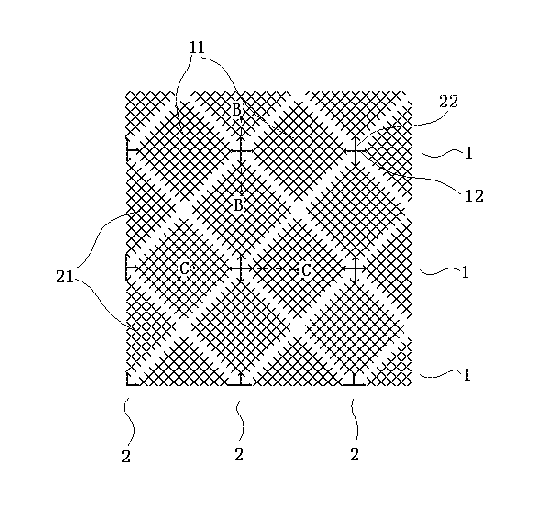
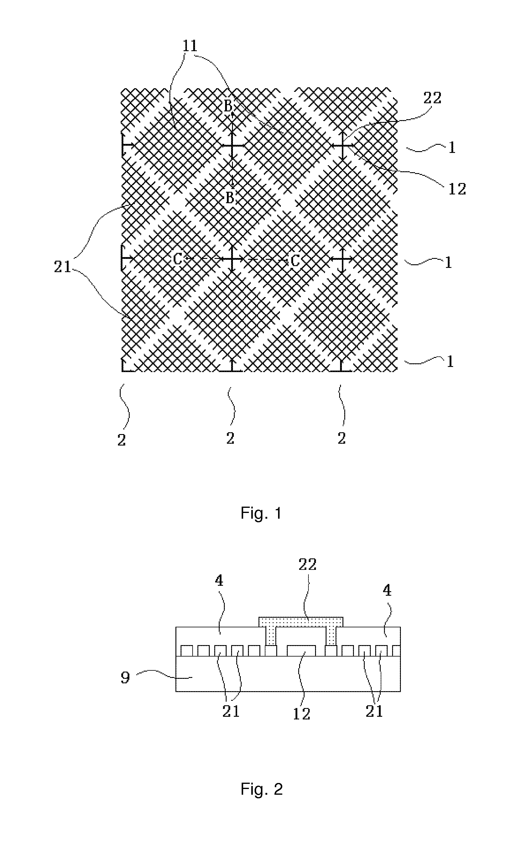
[0031]The present embodiment provides a touch substrate, as shown in FIG. 4 and FIG. 5, which comprises a base 9, and a plurality of first electrodes and a plurality of second electrodes, which intersect with each other, provided on the base 9.

[0032]Preferably, in the present embodiment, the driving electrodes 1 are first electrodes, and the sensing electrodes 2 are second electrodes, accordingly, first metal meshes are driving metal meshes 11, a first side strip is a driving side strip 13, second metal meshes are sensing metal meshes 21 and a second side strip is a sensing side strip 23.

[0033]The reason for the above setting is in that, the first electrodes are directly connected through the connection portions 12 and thus the resistance is small, and signals to be loaded on the driving electrodes 1 are relatively large, thus smaller resistance is required to increase the load capacity, therefore, such connected first electrodes are suitable for being the driving electrode 1. Certa...

embodiment 2

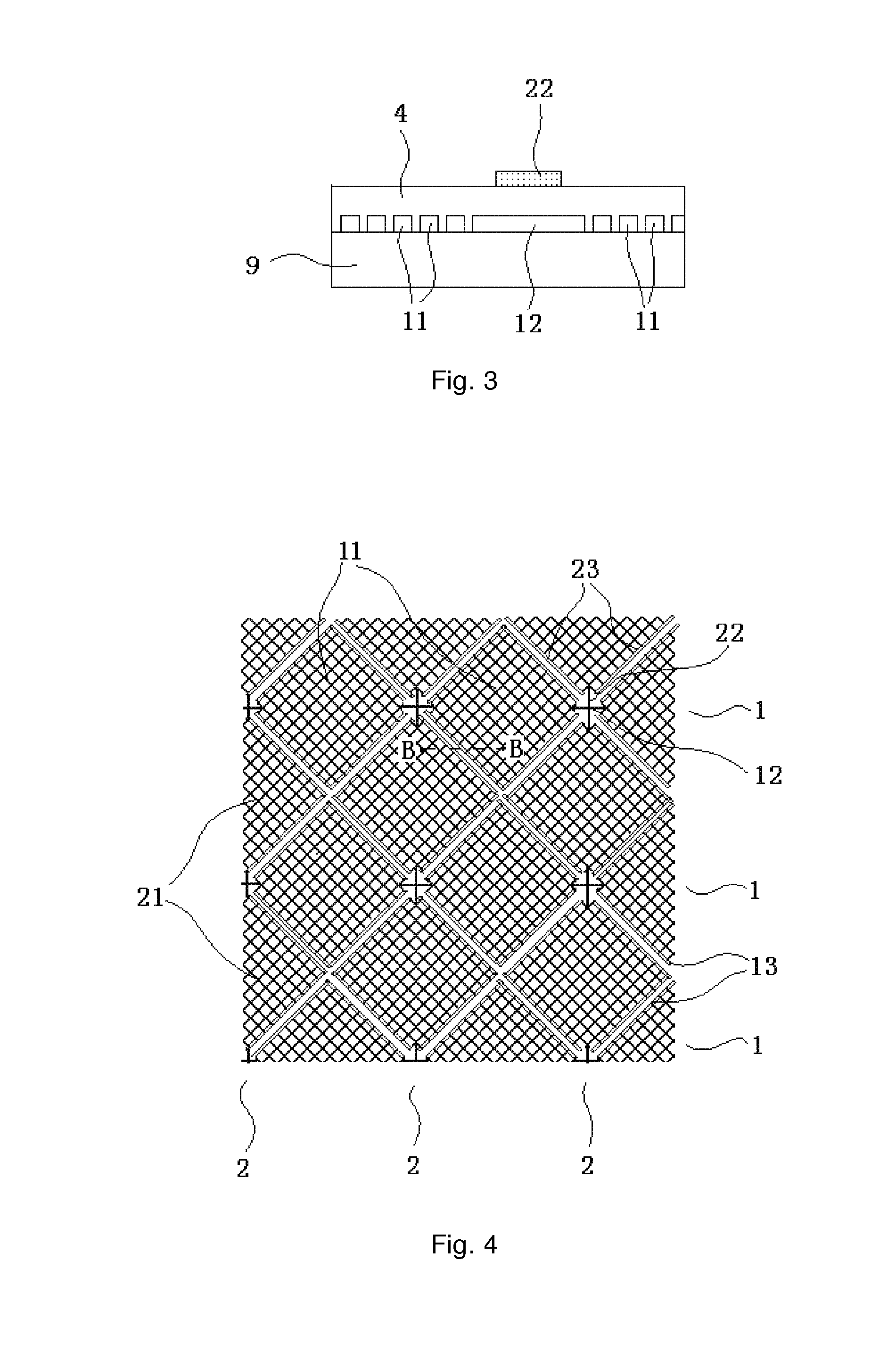
[0054]As shown in FIG. 6 and FIG. 7, the present embodiment provides a touch substrate, which comprises a similar structure of the touch substrate of the embodiment 1.

[0055]Unlike the touch substrate of the embodiment 1, in the present embodiment, the driving side strips 13 and the sensing side strips 23 are in the same layer as the connection portions 22, and as shown in FIG. 7, the driving side strips 13 are connected to the driving metal meshes 11 through vias in the insulation layer 4, and the sensing side strips 23 are connected to the sensing metal meshes 21 through vias in the insulation layer 4. While the driving side strips 13 and the sensing side strips 23 are in a different layer from that in the embodiment 1, the difference cannot be shown in the top diagram, thus the structure in FIG. 6 seems similar to that in FIG. 4.

[0056]Preferably, each side strip is respectively connected to all ends of the mesh lines at an edge of the metal mesh through vias, so that the connectio...

embodiment 3

[0060]The present embodiment provides a touch screen comprising any one of the above touch substrates. The touch screen may be any product or member with displaying function such as a liquid crystal panel, an electronic paper, an OLED panel, a mobile phone, a tablet computer, a TV, a monitor, a notebook computer, a digital photo frame, a navigator and so on.


PUM

PropertyMeasurementUnit
capacitanceaaaaaaaaaa
transparent conductiveaaaaaaaaaa
resistanceaaaaaaaaaa

Abstract

The present invention provides a touch substrate and a touch screen. The touch substrate comprises first electrodes and electrodes which intersect with each other, each first electrode includes a plurality of first metal meshes, adjacent first metal meshes are connected through a connection portion, each second electrode includes a plurality of second metal meshes, adjacent second metal meshes are connected through a connection bridge, the first metal meshes, the second metal meshes and the connection portion are in the same layer, and an insulation layer is provided between the layer in which the connection portion is located and the layer in which the connection bridge is located, at least a part of edges of the first metal mesh is provided with a first side strip thereat, the first side strip is adjacent to a corresponding second metal mesh and is connected to the first metal mesh.

Description

FIELD OF THE INVENTION[0001]The present invention relates to the field of the touch technology, and particularly to a touch substrate and a touch screen.BACKGROUND OF THE INVENTION[0002]The screen with touch function (touch screen) has been applied more and more widely. A capacitive touch screen is an important touch screen, the capacitive touch screen is provided with a plurality of driving electrodes (Tx) and a plurality of sensing electrodes (Rx) which intersect with each other, and a capacitance is generated at a position where the driving electrode and the sensing electrode are adjacent. The driving electrodes are loaded with driving signals in a scanning manner, and sensing signals are generated on the sensing electrodes accordingly. When touch happens, for example a human body or a touch pen closes to the touch region, the capacitance between the two kinds of electrodes in the touch region is influenced, and the sensing signal on the corresponding sensing electrode is changed...

Claims


Application Information

Patent Timeline
Patent Type & Authority Applications(United States)
IPC IPC(8): G06F3/044
CPCG06F3/044G06F2203/04112G06F2203/04111G06F3/0443G06F3/0446
Inventor HU, MINGZHANG, MINGZHANG, LEIGONG, WEIGANG
Owner BOE TECH GRP CO LTD
Why Eureka
Try Eureka